Every major technological leap begins with a machine that changes everything. The steam engine set the Industrial Revolution in motion. Today, the digital revolution is entering a new phase. Artificial intelligence is developing at unprecedented speed, but its true engine lies deeper: in the chips that power it, and in the lithography machines that print the tiniest patterns on those chips. The most advanced chipmaking tool in the world is now installed in imec’s cleanroom in Leuven, ready to define our technological future.
Sometimes technology emerges that pushes the world into a new era. After inventing the wheel, humans harnessed animal power to move goods and people. Centuries later, muscles were replaced by mechanical force with the arrival of the steam engine. The first prototype emerged in 1705, but it took sixty years before James Watt turned it into a practical, scalable machine. Another sixty years later, the Industrial Revolution was reshaping economies: steam engines powered factories, mines and transportation systems, including Europe’s early railways.
Technological progress doesn’t only change how we move – it also reshapes how we exchange ideas. When Johannes Gutenberg began casting individual metal letters around 1450, written knowledge could be reproduced faster than ever before. A century later, publishers scaled that process into early industrial publishing. Scientific treatises, multilingual bibles, atlases and dictionaries circulated widely across the continent, helping to knit together networks of scholars, merchants and artisans. This cultural and intellectual acceleration laid the groundwork for broader economic and scientific development across Europe.
What machine symbolizes progress today?
We may once again be living through a turning point, with technological breakthroughs arriving faster than society can absorb them. Artificial intelligence is reshaping how we process information at breathtaking speed. If we had to choose one machine that symbolizes this acceleration, what would it be? We may be tempted to think of the smartphones or laptops running our AI applications, or of the servers in data centers that train AI models. But these are merely the upper layers of a deeper technological foundation. Their computing power has grown explosively because the chips inside them have become vastly more capable. A modern smartphone contains billions of transistors and is millions of times more powerful than the computer that guided Apollo to the Moon.
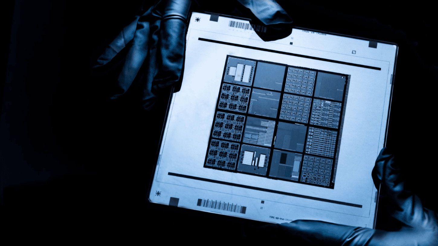
The relentless rise in performance rests on a simple principle: more transistors packed into a smaller area. Achieving this requires shrinking chip features to nanoscale through dozens of exquisitely controlled chemical and physical processes. One of those processes sets the ultimate limit of physics: lithography.
Photolithography uses light to print many microscopic patterns at once onto a light-sensitive material. The shorter the wavelength, the finer the “brush”. And because that brush keeps getting finer, the machines that control it have grown into some of the most complex systems ever built – so large they rival a city bus, packed with cutting-edge physics and engineering. If one machine embodies modern technological progress, this is it.
EUV lithography: painting with extreme ultraviolet light
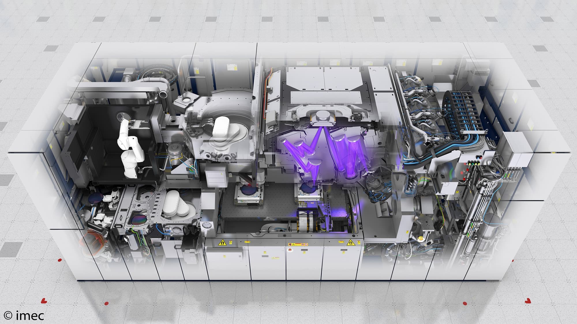
Today’s most advanced chips cannot be made without EUV lithography – extreme ultraviolet, referring to light with a wavelength of just 13.5 nanometers. Generating this light once seemed impossible. EUV does not exist naturally on Earth; the atmosphere would absorb it instantly, and it typically occurs only in the outer layers of the sun. To reproduce those conditions on Earth, scientists fire 100,000 droplets of molten tin per second into a vacuum chamber. A powerful laser hits each droplet several times at precisely the right moment, creating plasma that emits short bursts of EUV light.
And that is only the beginning. Because EUV is absorbed by nearly all materials, lenses are useless. Special mirrors – made from dozens of alternating layers of molybdenum and silicon, polished to near atomic smoothness – are needed to guide and focus the light. Integrating hundreds of such breakthrough technologies into a single working system was the true challenge. How do you keep a mirror clean while tin droplets explode nearby? How do you prevent reflected tin from damaging your laser?
ASML was the first – and remains the only – company capable of integrating all these elements into one machine. In 2006, after a decade of research, the first EUV demo tool arrived at imec’s cleanroom. In 2019, EUV was stable enough for industrial-scale chip production. Since then, EUV lithography has become the invisible engine beneath every advanced chip – and therefore beneath every modern AI application.
The next big thing: High NA EUV
Imec’s technology roadmap stretches to 2040 and synchronizes new materials, transistor architectures, interconnect technologies, and the next generation of lithography. Together, these advancements will push the semiconductor industry toward the ångström era — characterized by critical chip features at sub-nanometer scales. To cross that threshold, we need an even finer brush. EUV’s wavelength cannot realistically be shortened further. Fortunately, the Rayleigh criterion shows that resolution also depends on the numerical aperture (NA) of the optical system: higher NA means sharper focus and finer details.
Raising the NA from today’s 0.33 to 0.55 required an entirely new optical system – with mirrors twice as large, ten times heavier, and polished for months by ZEISS to atomic precision. The resulting High NA EUV tool is, quite literally, the next big thing: the size of a double-decker bus and weighing around 150 tons.
But the optics alone were not enough. Every downstream process – photoresist chemistry, etching, metrology – had to be reengineered to match the improved resolution. In imec and ASML’s joint High NA lab in Veldhoven, the full process chain was optimized. In 2024, imec demonstrated for the first time that High NA EUV achieves its theoretical resolution on a wafer – a world record. In 2025, imec and ASML deepened their strategic collaboration, ensuring that ASML’s latest machines, including the first High NA EUV tool, would be installed in imec’s cleanroom.
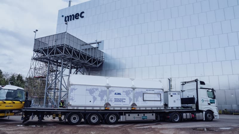
The first module of the High-NA EUV machine was transported to imec's 300 mm cleanroom in March 2026.
Why the ångström era begins here
Just as painters switch between broad brushes and ultrafine ones, chipmakers will continue to use today’s EUV machines for many layers — but High NA EUV unlocks the most demanding ones. Where current tools sometimes require multiple exposures, High NA can print the finest lines in a single stroke — simplifying the process flow, reducing defects, cutting costs, and lowering the overall carbon footprint. The higher resolution also restores creative freedom to chip designers, enabling two-dimensional circuit designs and smoother curves instead of only sharp angles which potentially lead to denser chips and shorter electrical paths.
Yet even the finest brush needs an atelier. A lithography system never stands alone: patterns come to life only when materials, etching processes, cleaning steps, mask and imaging technology, and metrology are perfectly aligned. That ecosystem is exactly what imec has built. In the world’s premier semiconductor R&D hub, chip manufacturers, materials suppliers, equipment suppliers, metrology experts, and chip designers co-develop new materials, refine process steps, reduce defects and update design rules.
Under the EU Chips Act, imec’s infrastructure is expanding even further. More than a hundred new semiconductor tools are being installed to create the NanoIC pilot line, strengthening Europe’s position in advanced semiconductor R&D for the decades ahead. The pilot line gives start-ups, universities and innovative companies access to cutting-edge chip technology to test ideas and accelerate new applications.

Left to right: Peter Vanoppen (ASML), Martin van den Brink (ASML), Luc Van den hove (imec), Matthias Diependaele (Minister President of the Flemish government), Patrick Vandenameele (imec) .
A window onto breakthroughs we cannot yet foresee
Whoever masters the brush that can draw at atomic scale will help shape the digital, medical and scientific progress of the coming decades. The arrival of a new generation of lithography technology therefore shifts not only the limits of what is technically possible on a chip, but also which scientific breakthroughs move within reach.
Consider the world of biosensors. Its progress depends on the precision with which we can engineer structures that operate at the scale of molecules. Nanopores are one example: tiny openings just a few nanometers wide in an ultrathin membrane. When a molecule, such as a DNA strand, passes through such a pore, the electrical current flowing through it changes. Those subtle variations reveal the order of the base pairs in the DNA. For DNA analysis, this already works surprisingly well. But for proteins — the tiny machines that determine what is happening inside our bodies — the process is far more complex.
To analyze millions of different proteins in parallel, you need thousands, potentially hundreds of thousands, of nanopores operating at once, each with precisely the same dimensions. Chip fabrication methods are proving to be the key to making that leap toward affordable, highly stable nanopores. Thanks to EUV lithography, it is now possible to reliably‑ produce large numbers of solid-state nanopores simultaneously. Imec has already succeeded in creating 10‑nanometer pores on a silicon wafer with exceptional uniformity.
Quantum chips based on semiconductor spin qubits impose similar demands: their devices require structures that are both extremely small and extraordinarily consistent. Around the world, researchers are exploring how lithography can help achieve that stability by defining patterns across entire silicon wafers without compromising the delicate coherence these qubits rely on. In other words: the more precisely we can make patterns at atomic‑scale tolerances, the closer we get to a scalable silicon-based quantum computer.
That is why this new generation of lithography is far more than a technological upgrade. It is a lever – a foundational technology that will drive the next wave of AI chips, enable a new generation of ultraprecise medical sensors, and even help push the development of silicon-based quantum computers forward. When James Watt made the steam engine stable and reliable, it became the engine of the Industrial Revolution. It did not change the world overnight, but it became the platform on which new industries emerged. The next generation of lithography tools may play that same role today: a foundation that unlocks breakthroughs across fields, including many we can scarcely imagine today.
This content is only visible on the desktop version of this website.