
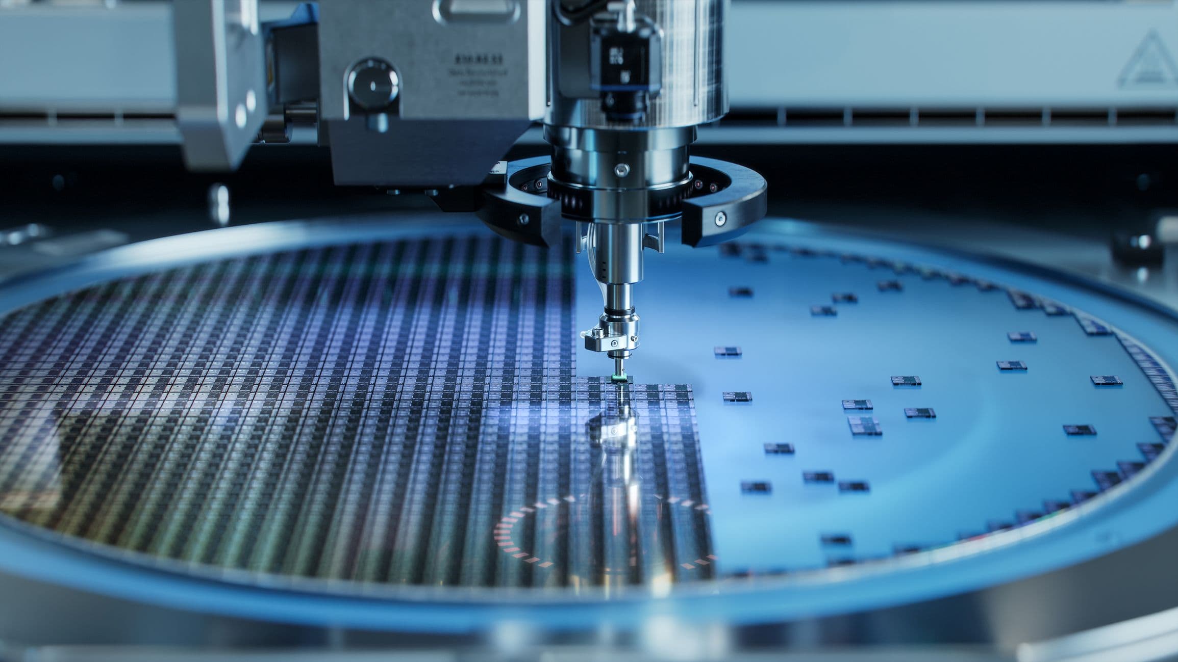
Custom chip manufacturing
Go from idea to scalable and reliable semiconductor manufacturing with IC-Link.
IC-Link provides customized solutions for innovative chip manufacturing, built on imec’s semiconductor expertise. Next to silicon production, the division includes services spanning from design through packaging, assembly, qualification, and supply chain management.
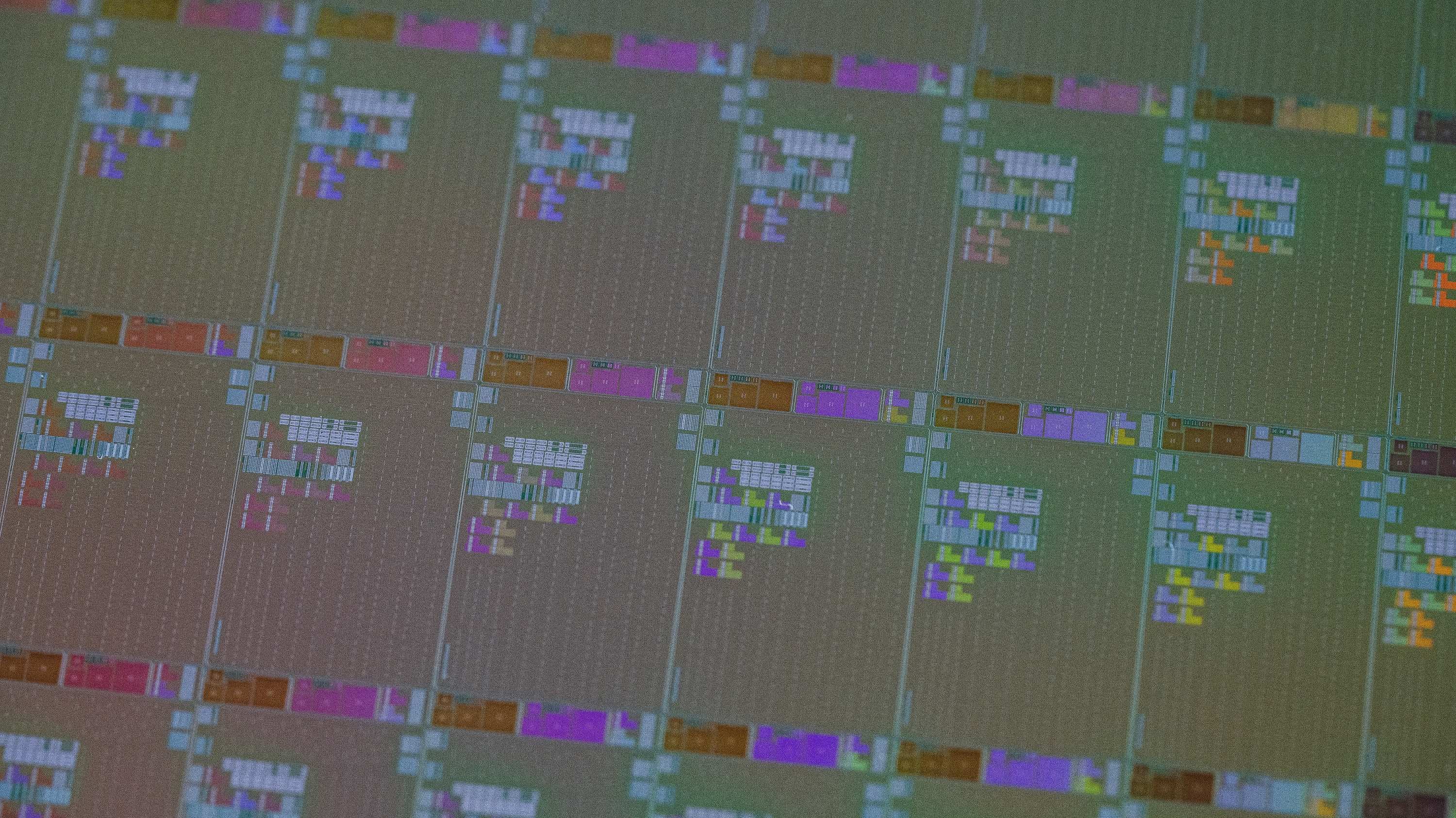
Technologies range from ASICs in CMOS, including the most advanced commercially available nodes, to imec-developed integrated photonics, custom wafer processes, and 2.5D and 3D packaging. This portfolio continually expands with new platforms fresh from R&D once they are commercially validated.

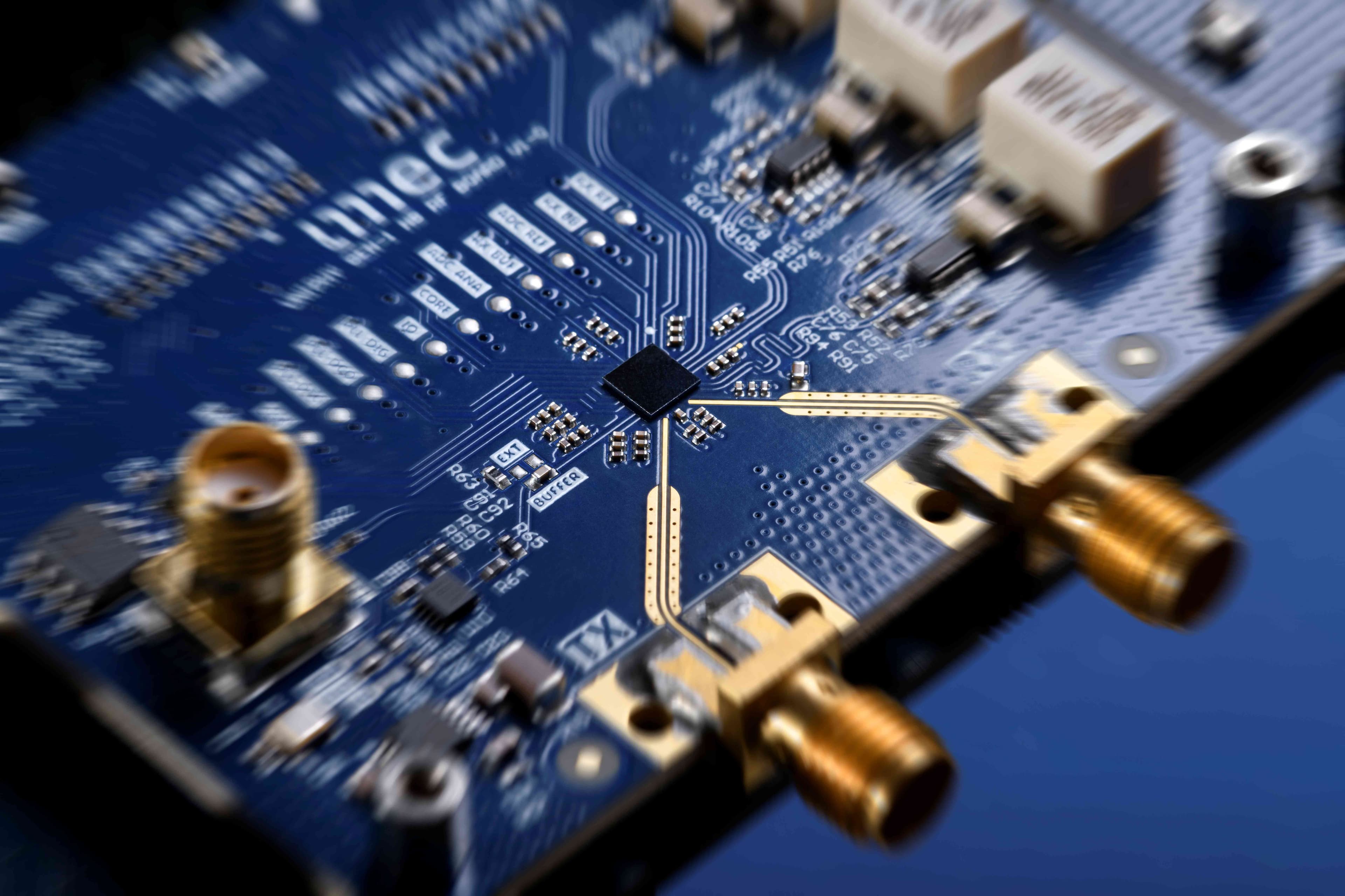
ASIC services
A custom ASIC allows you to differentiate your product through higher performance, smaller form factor, better IP protection, and more.
IC-Link’s CMOS ASIC offering includes:
- A wide range of technology nodes down to N2
- Partnerships with commercial foundries, including TSMC as Value Chain Alliance (VCA) member
- Flexible business models including full turnkey
- Design capabilities across digital, analog and mixed signal
- Packaging solutions including 2.5D/3D design and production
- Testing development, qualification and supply chain management services to serve high-volume customers
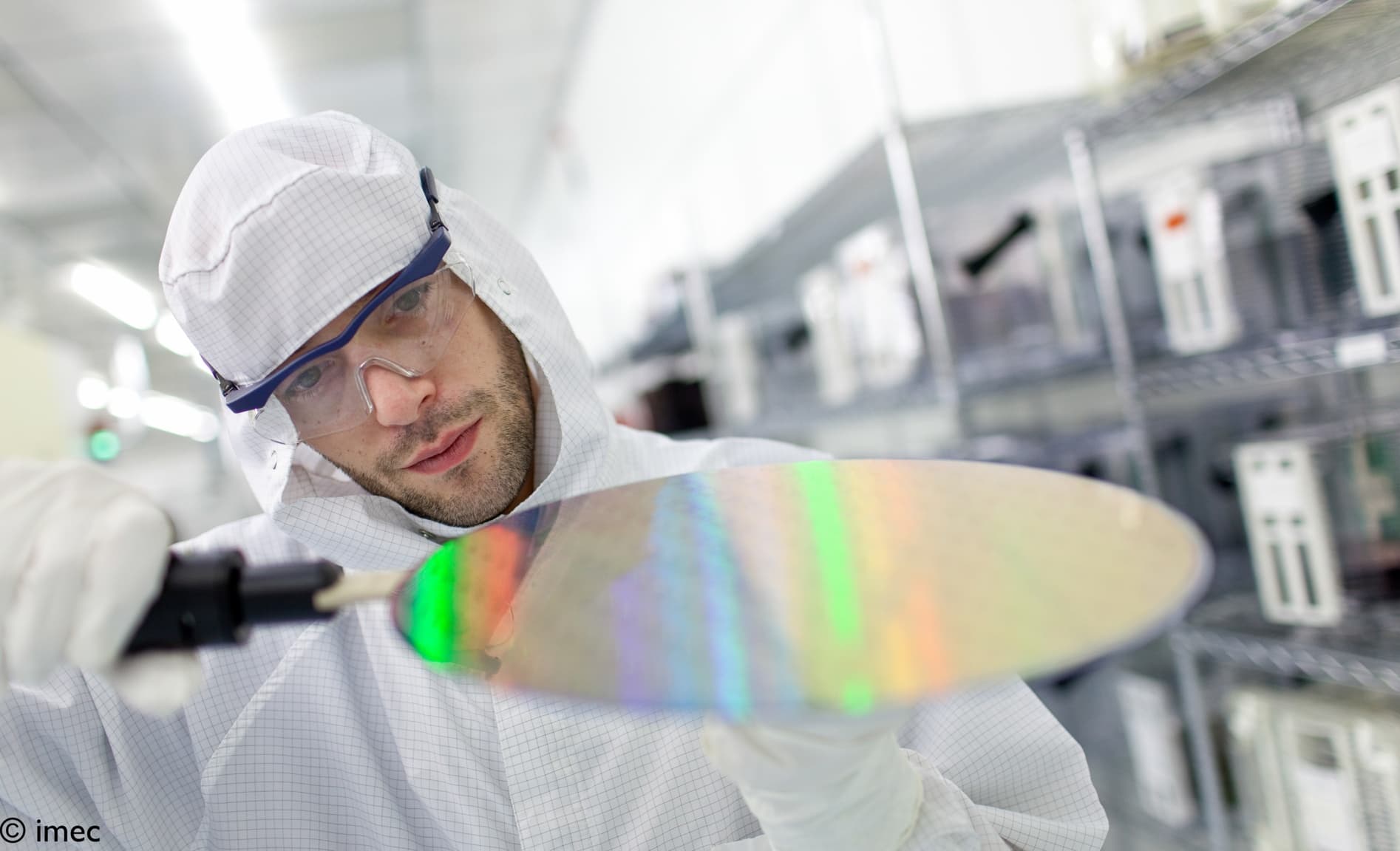
PIC services
Differentiate your application by harnessing the high performance and low power consumption of a silicon photonics integrated circuit (PIC).
IC-Link's 200mm silicon photonics platform, iSiPP200 offering includes:
- A complete, state-of-the-art PDK, regularly updated with new advancements, coming from imec’s leading photonics research program
- Flexible volumes thanks to foundry access
- Service model to go from idea to production
- Additional photonics platforms on the roadmap
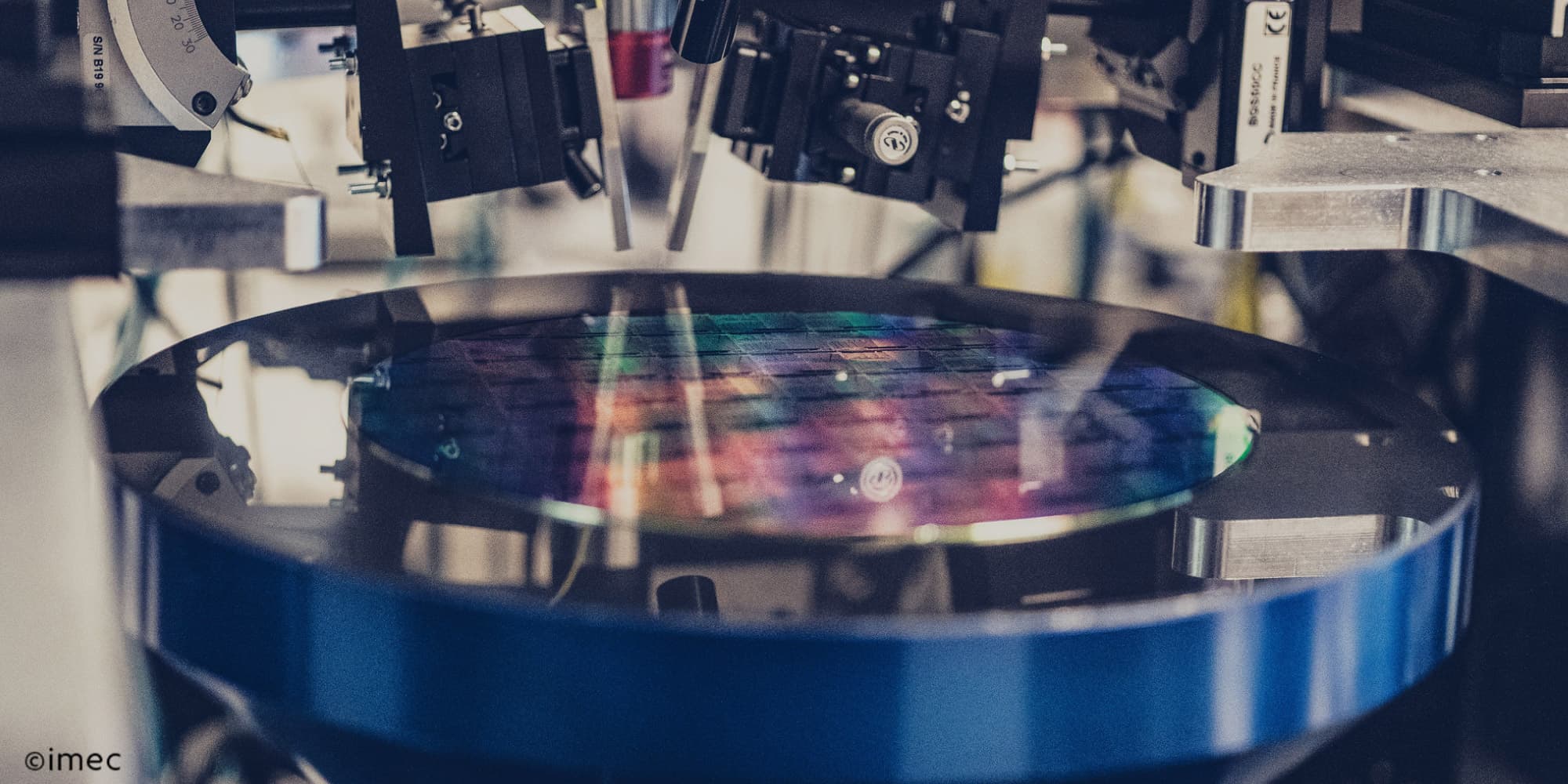
Custom wafer process services
Get access to manufacturing capabilities without a standard flow. These include:
- Custom-developed imagers and detectors, from design to production based on imec’s R&D
- Fine-resolution wafers using state-of-the-art lithography tools
- CMOS post-processing: unique capabilities that can be combined with photonics, advanced lithography, and more
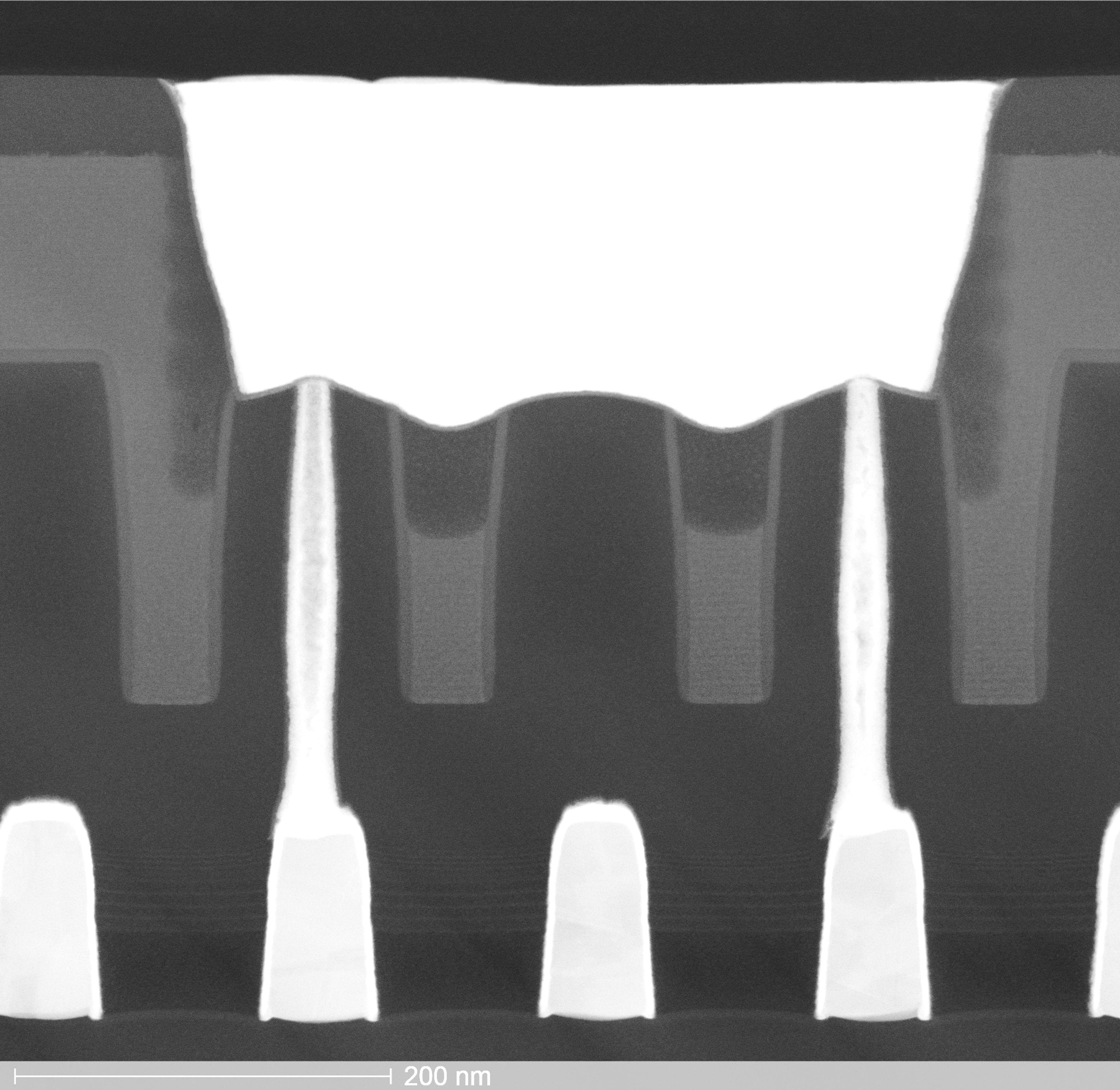
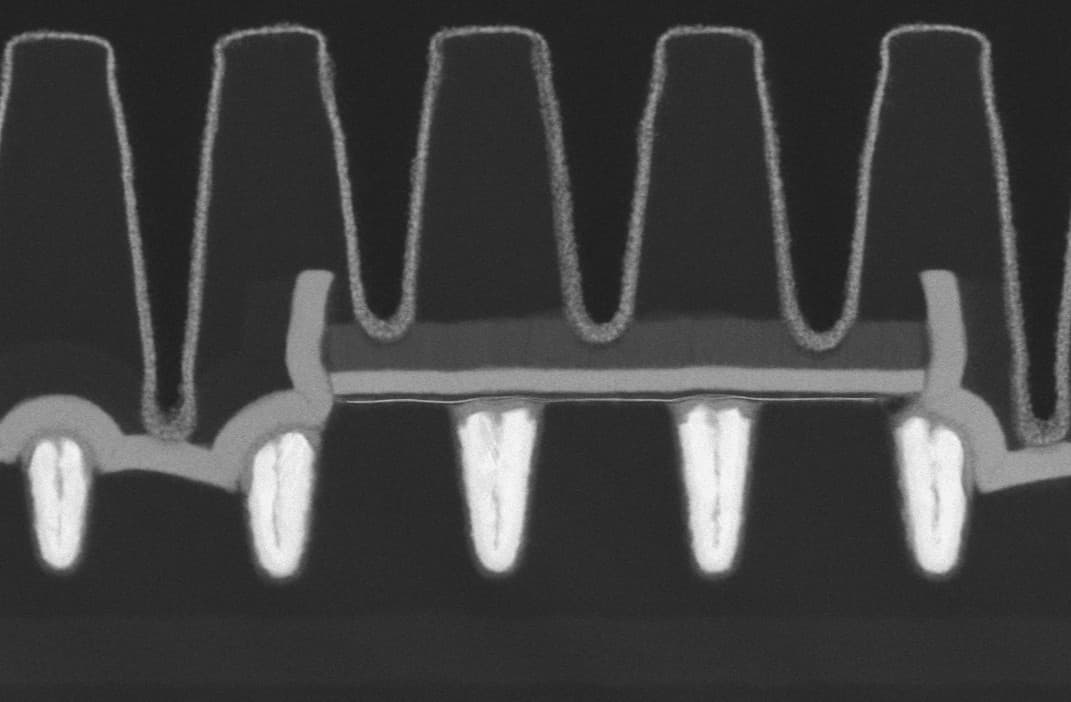
Example project: From circuit design and specialty Si-processing to seeing atoms
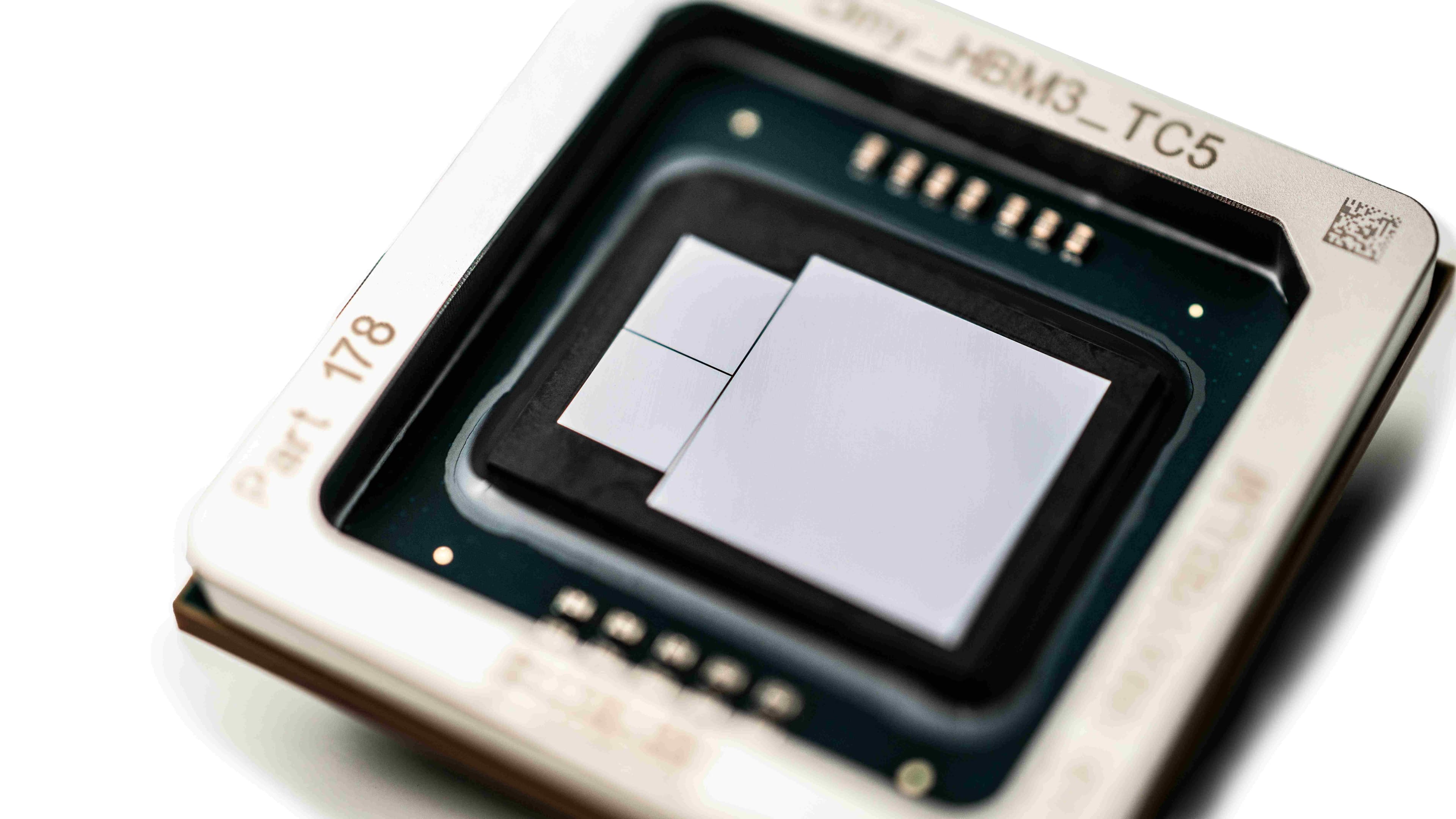
Advanced packaging services
A broad range of mainstream to advanced packaging techniques is available through our ASIC partners. This is complemented by selected imec-developed 2.5D and 3D packaging services.
Examples include:
- 2D packaging: ball grid array (BGA), land grid array (LGA), wafer-level chip-scale packaging (WLSCP), multi-chip module (MCM), system in package (SiP)
- 2.5 packaging: via packaging partners, imec-developed solution coming in 2026
- 3D packaging: via packaging partners, imec solution under development
Press releases
13 July 2026
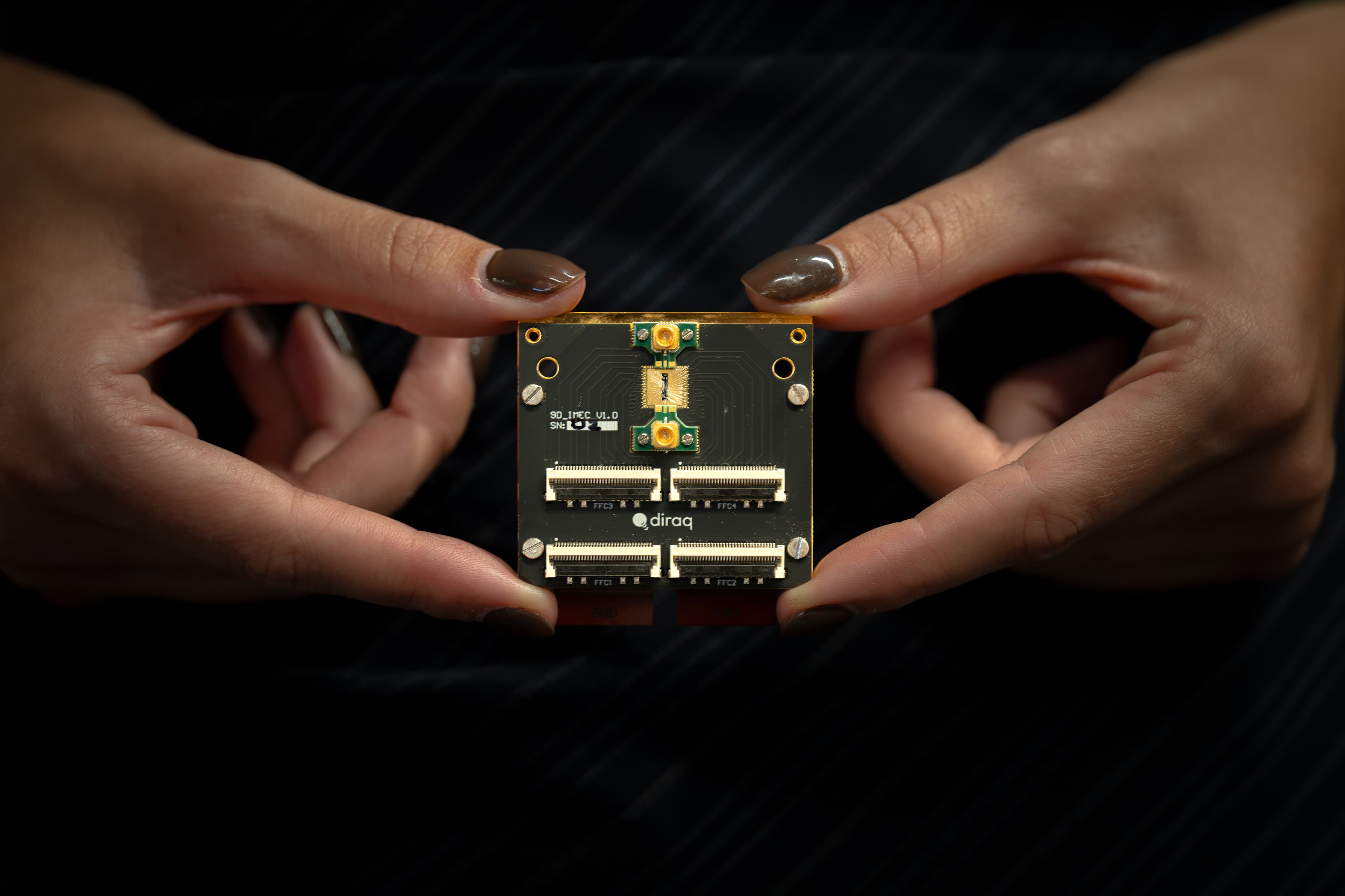
Result shows that industrial semiconductor manufacturing can support the scaling of silicon quantum processors beyond the two-qubit regime.

Press releases
17 June 2026
As AI workloads drive a steep increase in memory capacity, imec explores ferroelectric memory technologies to address the cost and density constraints of classical DRAM.
Press releases
16 June 2026
The new integration approach implements sub-100nm self-aligned through-Si via connections, enabling low-resistance and low-leakage front-to-back connections with good overlay performance
Press releases
15 June 2026
Novel 300mm integration approach for 2D-material based devices enables scaled n and pFETs with 50nm contacted poly pitch
Press releases
9 June 2026
Building on this, imec further demonstrates the first full transceiver architecture compliant with IEEE 802.15.4ab, delivering up to a 32x improvement in ranging performance through combined receiver, transmitter, and IEEE 802.15.4ab standard innovations

Press releases
28 May 2026
Through their continued collaboration, imec and EV Group (EVG) are focusing on advancing the overlay performance required for advanced logic-to-logic and memory-to-logic tier stacking.

Press releases
19 May 2026
The most advanced lithography system, crucial for future advanced memory and computer chips, will play a key role in scaling up quantum technology

Press releases
12 May 2026
The feasibility of processing a charge coupled device (CCD) in a 3D NAND-like architecture paves the way for a cost-effective, high-bit-density memory solution to address the memory wall for AI specific workloads

Press releases
12 May 2026
Expands global ASIC services expertise and aims to take on the industry’s most advanced AI, HPC, mobile and automotive projects


Press releases
18 March 2026
A major milestone in propelling industry into the ångström era

Subscribe to our thematic newsletters