Introduction
Partners within the European ‘PowerBase’ project are developing the next-generation of energy-saving chips (or power devices) based on materials such as gallium nitride (GaN). Under the coordination of Infineon, they will prepare these semiconductors for mass industrial use in smartphones, laptops, servers and many other applications. Among the 39 project partners is imec. Its main role: looking beyond the traditional substrate technologies in order to improve the crystal quality of the GaN layer.
GaN: efficient power conversion
Power semiconductors play a key role in the power conversion in electronic devices such as smartphones, computers, servers and lighting systems, and photovoltaics. Built into the device’s charger or power supply, they convert the mains voltage from the wall socket according to the needs of the device. A major requirement is keeping the amount of energy lost during conversion (usually in the form of waste heat) to an absolute minimum. Traditionally, Si is used as the base materials for power devices. But with its higher breakdown strengths, faster switching speeds and lower on-resistance, power devices based on the wide-bandgap semiconductor material GaN can convert power far more efficiently than Si-based chips. In AlGaN/GaN HEMTs for example, a very low on-resistance and high switching speed is obtained due to the two-dimensional electron gas (2DEG) which is formed spontaneously at the AlGaN/GaN interlayer.
In the future, a new generation of GaN-based power semiconductors is expected to reduce the amount of energy lost in power supplies even further. They will also enable miniaturization in many applications where size matters. For example, chargers and power supplies will become significantly smaller and lighter. An important step on the way to a laptop power supply with the size of a matchbox or conveniently integrated into a power plug.
The PowerBase project
39 partners from nine European countries have joined the PowerBase project to develop these next-generation energy-saving chips. The PowerBase research focus includes intensive material and reliability research to improve the quality and lengthen the service life of GaN-based semiconductors. Plans also foresee the establishment of pilot lines for 200mm wafers to manufacture GaN-based power components in a high-volume industrial production environment. The project involves the entire value chain, covering expertise in raw materials research, process innovation, assembly innovation, pilot lines up to various application domains.
Keeping Europe at the forefront
The overall research activities in the project are coordinated on a European-wide basis in order to make the new semiconductors ready for mass industrial use at globally competitive cost levels. Infineon Austria leads the PowerBase project, which kicked off in May 2015. It is a private-public partnership in which investments from industry, funding from individual countries and the support of the ECSEL (Electronic Components and Systems for European Leadership) Joint Undertaking are being applied. The 87 million euro project volume and the participation of so many partners give an idea of the great importance the EU is attaching to the project. PowerBase, set to run until 2018, will strengthen and expand Europe’s status as a center of expertise for the development and production of innovative power electronics.
Imec looks beyond traditional substrate technologies
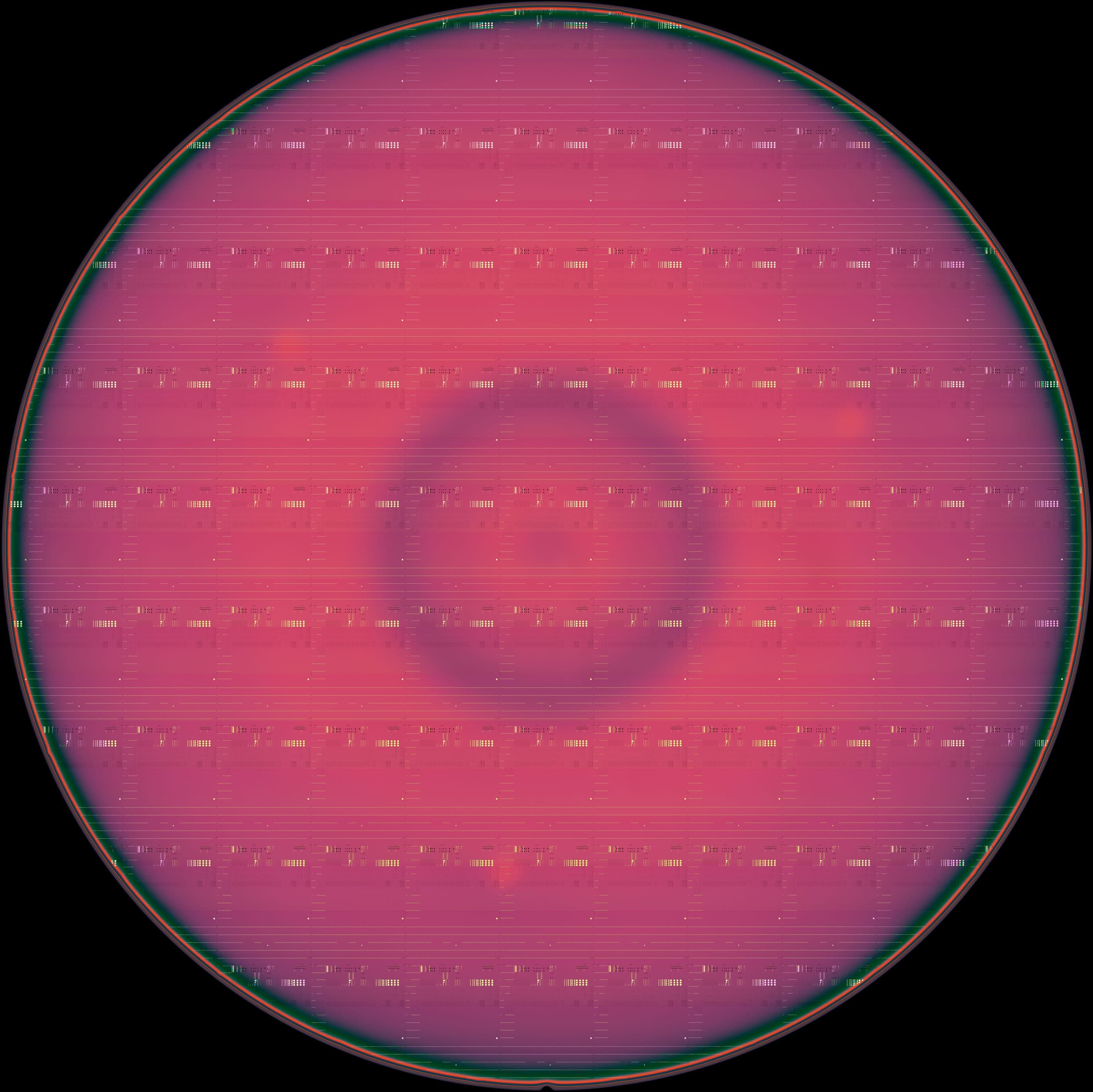
While SiC substrates are often preferred for easier thermal management, Si substrates have become very attractive for GaN growth because of their larger wafer diameter (200mm and higher) and lower costs perspectives. The growth of GaN on Si is however very challenging and is seen as a possible stumbling block for further improving on the current generation of GaN-based power devices. The lattice mismatch between Si and GaN and the thermal expansion mismatch during growth or cool down can lead to film cracking or wafer bowing, and can generate a high density of defects. The wafer bow also increases with increasing wafer sizes which makes up-scaling difficult.
Within the PowerBase project, imec will therefore look into new substrate approaches that provide a better (Al)GaN crystal quality and lower wafer bow. Novel substrates (such as AlN and Mo substrates) as well as alternative growth techniques will be explored. The target diameter for the advanced substrates is 200mm, and their compatibility with the pilot line activities within the PowerBase project will be assessed.
EpiGaN partners to push the boundaries of commercial state-of-the-art products
It is essential that the performance of these new developments can be benchmarked against state-of-the-art existing GaN-on-Si substrates that are produced on an industrial scale. For this task, imec’s spin-off EpiGaN comes into the picture. As a partner in the PowerBase project, EpiGaN – a supplier of GaN-on-Si wafers – will continuously push the boundaries of its state-of-the-art GaN-on-Si epitaxial technology for power switching. They will act as a benchmark for the novel substrates developed by imec. As a result of the project, EpiGaN will also have established the technology to supply low-cost 600V GaN-on-Si on 200mm substrates to Europe and to the world.
Partners within the European ‘PowerBase’ project are developing the next-generation of energy-saving chips (or power devices) based on materials such as gallium nitride (GaN). Under the coordination of Infineon, they will prepare these semiconductors for mass industrial use in smartphones, laptops, servers and many other applications. Among the 39 project partners is imec. Its main role: looking beyond the traditional substrate technologies in order to improve the crystal quality of the GaN layer.
GaN: efficient power conversion
Power semiconductors play a key role in the power conversion in electronic devices such as smartphones, computers, servers and lighting systems, and photovoltaics. Built into the device’s charger or power supply, they convert the mains voltage from the wall socket according to the needs of the device. A major requirement is keeping the amount of energy lost during conversion (usually in the form of waste heat) to an absolute minimum. Traditionally, Si is used as the base materials for power devices. But with its higher breakdown strengths, faster switching speeds and lower on-resistance, power devices based on the wide-bandgap semiconductor material GaN can convert power far more efficiently than Si-based chips. In AlGaN/GaN HEMTs for example, a very low on-resistance and high switching speed is obtained due to the two-dimensional electron gas (2DEG) which is formed spontaneously at the AlGaN/GaN interlayer.
In the future, a new generation of GaN-based power semiconductors is expected to reduce the amount of energy lost in power supplies even further. They will also enable miniaturization in many applications where size matters. For example, chargers and power supplies will become significantly smaller and lighter. An important step on the way to a laptop power supply with the size of a matchbox or conveniently integrated into a power plug.
The PowerBase project
39 Partners from nine European countries have joined the PowerBase project to develop these next-generation energy-saving chips. The PowerBase research focus includes intensive material and reliability research to improve the quality and lengthen the service life of GaN-based semiconductors. Plans also foresee the establishment of pilot lines for 200mm wafers to manufacture GaN-based power components in a high-volume industrial production environment. The project involves the entire value chain, covering expertise in raw materials research, process innovation, assembly innovation, pilot lines up to various application domains.
Keeping Europe at the forefront
The overall research activities in the project are coordinated on a European-wide basis in order to make the new semiconductors ready for mass industrial use at globally competitive cost levels. Infineon Austria leads the PowerBase project, which kicked off in May 2015. It is a private-public partnership in which investments from industry, funding from individual countries and the support of the ECSEL (Electronic Components and Systems for European Leadership) Joint Undertaking are being applied. The 87 million euro project volume and the participation of so many partners give an idea of the great importance the EU is attaching to the project. PowerBase, set to run until 2018, will strengthen and expand Europe’s status as a center of expertise for the development and production of innovative power electronics.
Imec looks beyond traditional substrate technologies
While SiC substrates are often preferred for easier thermal management, Si substrates have become very attractive for GaN growth because of their larger wafer diameter (200mm and higher) and lower costs perspectives. The growth of GaN on Si is however very challenging and is seen as a possible stumbling block for further improving on the current generation of GaN-based power devices. The lattice mismatch between Si and GaN and the thermal expansion mismatch during growth or cool down can lead to film cracking or wafer bowing, and can generate a high density of defects. The wafer bow also increases with increasing wafer sizes which makes up-scaling difficult.
Within the PowerBase project, imec will therefore look into new substrate approaches that provide a better (Al)GaN crystal quality and lower wafer bow. Novel substrates (such as AlN and Mo substrates) as well as alternative growth techniques will be explored. The target diameter for the advanced substrates is 200mm, and their compatibility with the pilot line activities within the PowerBase project will be assessed.
EpiGaN partners to push the boundaries of commercial state-of-the-art products
It is essential that the performance of these new developments can be benchmarked against state-of-the-art existing GaN-on-Si substrates that are produced on an industrial scale. For this task, imec’s spin-off EpiGaN comes into the picture. As a partner in the PowerBase project, EpiGaN – a supplier of GaN-on-Si wafers – will continuously push the boundaries of its state-of-the-art GaN-on-Si epitaxial technology for power switching. They will act as a benchmark for the novel substrates developed by imec. As a result of the project, EpiGaN will also have established the technology to supply low-cost 600V GaN-on-Si on 200mm substrates to Europe and to the world.
Novel isolation technologies
Imec will also look into alternative techniques for the electrical isolation in GaN-on-Si power devices. Today, isolation in GaN-on-Si devices comprises of lateral and vertical isolation. While lateral isolation is provided by an isolation implant, vertical isolation is realized by the high-resistive buffer. In addition, one of the terminals, typically the source, is connected to the substrate to make sure it is not floating. This configuration however brings along limitations for some convertor topologies that consist of high-side switches (with the source at a high potential) and low-side switches (with the source at a low potential). With traditional means, those two switches cannot be co-integrated as the substrate can only be referenced to a single potential at a time. Therefore, imec will look into alternative isolation modules that allow to increase the level of integration.

This project has received funding from the Electronic Component Systems for European Leadership Joint Undertaking under grant agreement No 662133. This Joint Undertaking receives support from the European Union’s Horizon 2020 research and innovation programme and Austria, Belgium, Germany, Italy, Slovakia, Spain, United Kingdom and the Netherlands.
More info:
More about these topics:
Published on:
19 December 2016


