A large consortium of industrial and academic players will for the first time in Europe introduce silicon carbide (SiC) and gallium nitride (GaN) in the power electronic circuits and charging infrastructure of electrified vehicles – including electric and hybrid cars. This way, they will help increasing the driving range, and reducing the energy consumption and price of the vehicles. Steve Stoffels, project manager at imec, and Stefaan Decoutere, program director GaN technology at imec, shed light on this HiPERFORM project, and clarify imec’s role.
Joint European effort aims for more energy efficient electric cars
With a share of approximately 23%, the transportation system in Europe contributes significantly to the total Greenhouse gas emissions and global climate warming. The automotive industry therefore faces the tremendous challenge of reducing emissions of CO2, which is one of the main Greenhouse gases emitted from vehicles. The massive introduction of affordable and energy-efficient electric vehicles is a key measure to help meet the ambitious CO2 targets and realize a decarbonized transportation system.
In this context, a large number of European industrial companies and research institutes, including imec, have teamed up to introduce for the first time wide-bandgap technologies in the power electronic circuits and charging infrastructure of electric cars.
Within the HiPERFORM project, they will help reducing a significant amount of the energy losses and sizes of the electronic power circuits. For example, if only 2% of the cars will use these new technologies, direct energy savings of 12.83TWh per year can be expected. These advanced power electronic technologies will not only allow for longer driving ranges and less energy consumption, they are also expected to contribute to the price reduction of electric cars.
Why wide-bandgap materials?
Electric cars need efficient power electronic circuits to convert electrical energy from different voltage levels, or from AC to DC and vice versa. Power electronic circuits can be found in various parts of the electric car. For example, they convert the AC power from the charging point or power socket to a battery-compatible DC power level, they transmit high levels of power from the battery towards the electromotor, or they convert and distribute power towards the heating, cooling and lighting systems within the car. Power electronic circuits are also needed in test systems for the car’s drivetrain – systems that allow to test the batteries or electromotors in a most efficient way.

Electric cars rely on power electronic circuits for various functions. What if we could make these better by using new materials, such as SiC and GaN?
At the heart of these power electronic circuits are power electronic components such as switches and inverters. Today, these components are made from standard Si semiconductors. But through the years, wide-bandgap materials such as SiC and GaN have been introduced, outperforming Si in many ways. Power electronic components made from these materials can operate at higher switching frequencies and at higher temperatures, leading to higher energy efficiency in electric motors and hybrid drive systems. These unique properties also allow to shrink the dimensions of the other power circuit components, such as cooling systems and passive elements – leading to more compact and light-weight power electronic systems.
The HiPERFORM project partners will use these wide-bandgap materials to research and develop highly-efficient, reliable power electronic components, and introduce them in the drivetrain, chargers and test systems of the next-generation electric and hybrid cars. Both SiC and GaN based components will be explored. SiC, being able to sustain higher voltages compared to GaN, will most probably be used for the most ‘demanding’ applications, such as the car’s drivetrain.
How is imec contributing?
Imec is involved in the study of novel materials and processes that will allow an increase of the reliability and a decrease of the cost of GaN switches.
More particularly, imec is developing novel substrate materials and corresponding epitaxy processes for growing GaN, and – together with Fraunhofer FEP – looks into more efficient ways of depositing the GaN buffer layer.
Poly-AlN substrates for improved reliability
Reliability is a key requirement for automotive applications. For power electronic components, this requirement translates into high breakdown voltages of 1.2kV. But today’s GaN-based components – which are typically fabricated on Si substrates because of the low- cost perspectives – cannot withstand voltages higher than 650V.
This limitation is basically related to the lattice mismatch between Si and GaN, and, even more importantly, to the thermal expansion mismatch during growth or cool down. The latter plays an extremely important role due to the high temperatures at which the GaN buffer is grown. To compensate for this mismatch, buffer layers (based on (Al)(Ga)N) are grown in between Si and GaN, which act as stress compensation layers. The thicker these buffer layers, the higher the breakdown voltage.
But with 200mm GaN-on-Si, there is a limitation to the thickness with which the buffer layers can be grown. With increased thickness, cracking of the AlN/GaN films and wafer bowing may generate a high density of defects, causing yield losses when mechanically handling these wafers. This puts a limit on the maximum achievable thickness and thus breakdown voltage of the buffer. On 200mm GaN-on-Si, reaching breakdown voltages above 650V is therefore extremely challenging.
To scale up voltages, imec proposes a novel substrate material for growing GaN: poly-aluminum-nitride (poly-AlN). The thermal expansion coefficient of this material better matches the thermal expansion coefficient of GaN. Theoretically, thicker buffer layers can be grown – allowing for higher operating voltages and hence increased reliability. Simultaneously, the epitaxy process needs to be adopted considerably from the traditional approaches for GaN-on-Si, in order to leverage the benefits of the poly-AlN substrate.
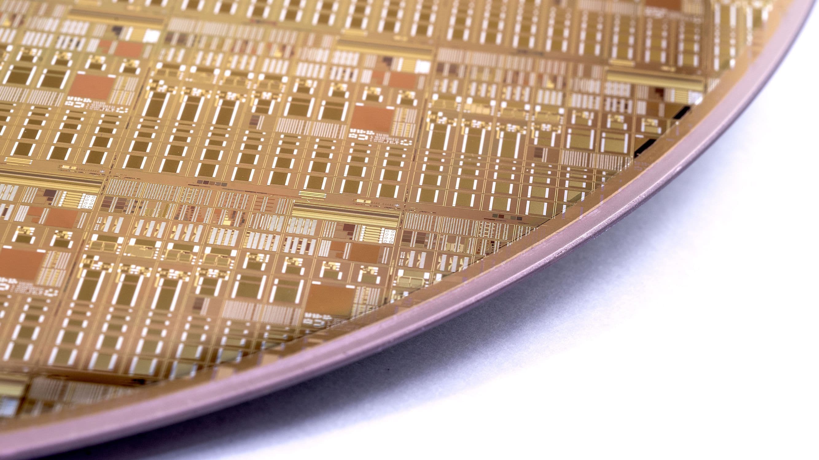
GaN power components on a 200mm poly-AlN substrate
Within a previous ECSEL project, named PowerBase, imec had already demonstrated the potential of the poly-AlN substrates, which are offered by Qromis. In HiPERFORM, the goal is to develop 1.2kV rated GaN buffers on these substrates. Imec has developed a proprietary epitaxial buffer scheme for growing the device stack on the poly-AlN substrate. Initial results look very promising, with breakdown voltages already as high as 900-1000V. The buffer consists of an AlN nucleation layer (a template), an AlGaN transition layer and a superlattice structure of GaN/AlN.
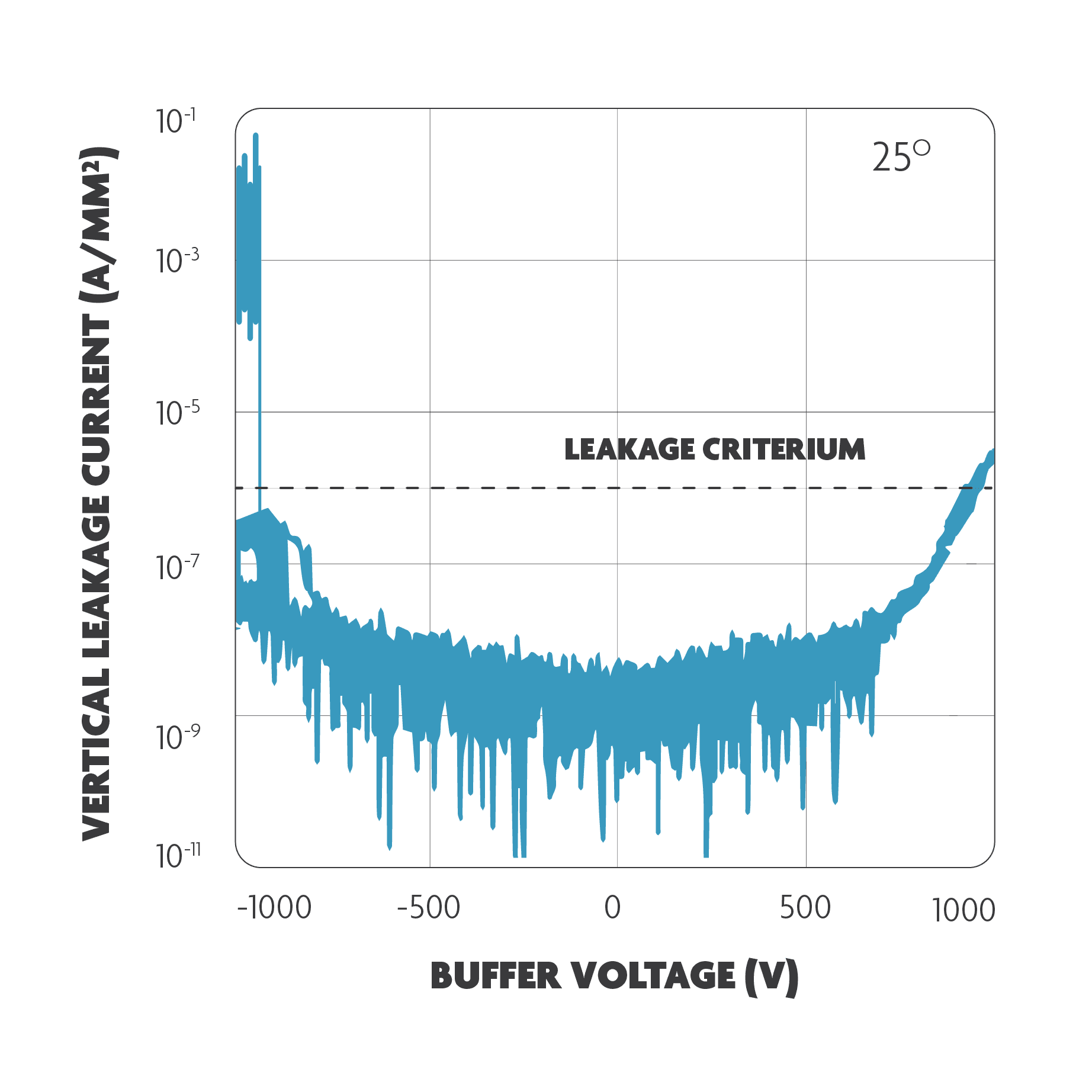
Graph illustrating high buffer breakdown voltages obtained on poly-AlN substrates with the imec proprietary buffer scheme
Sputtered AlN templates and buffers for cheaper production
Traditionally, the layers of the GaN buffer are grown by metal-organic chemical vapor deposition (MOCVD). The MOCVD process however significantly adds to the final cost of the GaN components. Therefore, Fraunhofer FEP is developing a novel sputter system for more efficiently growing specific layers of the buffer, with imec supporting the development of the epitaxial layers with this tool. This unique way of growing GaN buffer layers is expected to allow for faster growth rates, lower growth temperatures, a smaller number of material resources and the ability to move to larger substrates.
Although accurate calculations of the actual cost savings will be carried out in the course of the project, a first estimation predicts a long-term cost reduction of 40% in comparison with existing samples of these innovative GaN switches. Initially, the new system will be used for sputtering the AlN nucleation layer. Later on, it will be investigated if the new technique can be deployed for growing other layers of the buffer.
The outcome of the project will in the first place have a positive impact on the next generation of highly efficient electric cars. In addition, the results will strengthen the position of GaN in the (automotive) market with respect to competing technologies.
HiPERFORM kicked off in May 2018, and runs for three years under the coordination of AVL, Germany. This project has received funding from the ECSEL Joint Undertaking (JU) under grant agreement No 783174. The JU receives support from the European Union’s Horizon 2020 research and innovation programme and Austria, Spain, Belgium, Germany, Slovakia, Italy, the Netherlands, Slovenia.
Want to know more?
- ‘European ‘PowerBase’ to explore the next-generation power devices’, imec magazine.
- Visit imec’s website on GaN power devices
- Visit the website of the HiPERFORM project.

Steve Stoffels received the M.Sc. (magna cum laude) degree in applied physics from the University of Eindhoven, Eindhoven, the Netherlands, in 2001, and the Ph.D. degree from the Katholieke Universiteit Leuven, Belgium, in 2010. He is currently a device engineer with imec, Leuven, where he is involved in the research and development of high-power GaN technology. He is also project manager for funded projects in GaN. Since 2017 he is member of the IRPS technical committee for wide bandgap semiconductors.

Stefaan Decoutere received the M.Sc. degree in electronic engineering and the Ph.D. degree from the Katholieke Universiteit Leuven, Belgium, in 1986 and 1992 respectively. He is with imec, Leuven, since 1987, where he started in high-voltage BCD technology development. From 1992 till 1997, he was in charge of the development of high-speed BiCMOS and SiGe HBT technologies. In 1998, he became the head of the mixed signal/RF technology group in imec. Since 2010 he manages the GaN power device technology development, and in 2015 he became the director of the GaN technology program.
More about these topics:
Published on:
26 February 2019


