
Interested in our new sensor?
Following its initial announcement at the 2024 Small Satellite conference, imec’s most advanced hyperspectral sensor for Earth observation and industrial applications has officially transitioned from the research and development phase to broader adoption by imaging system developers and application partners.
Designed, optimized, and manufactured in imec’s world-class cleanroom facilities, this line-based (linescan) hyperspectral sensor is now ready for purchase by camera builders and satellite constellation developers.
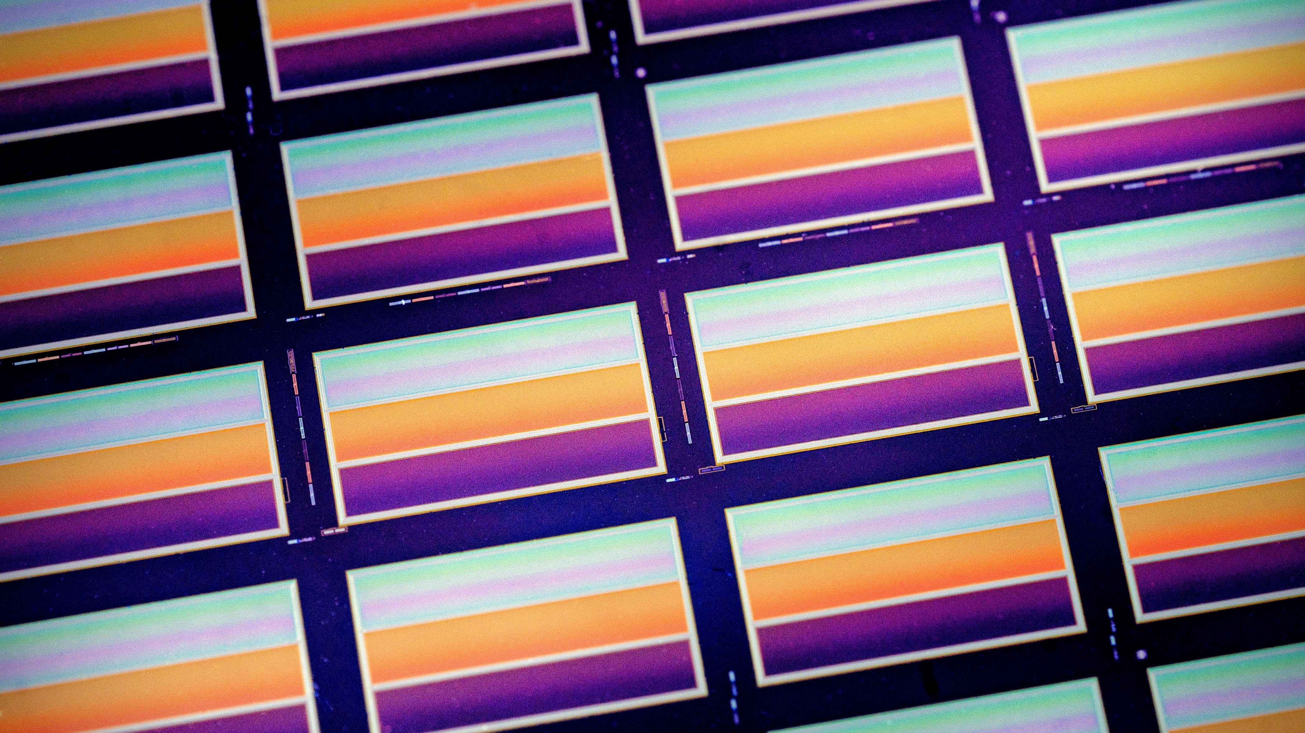
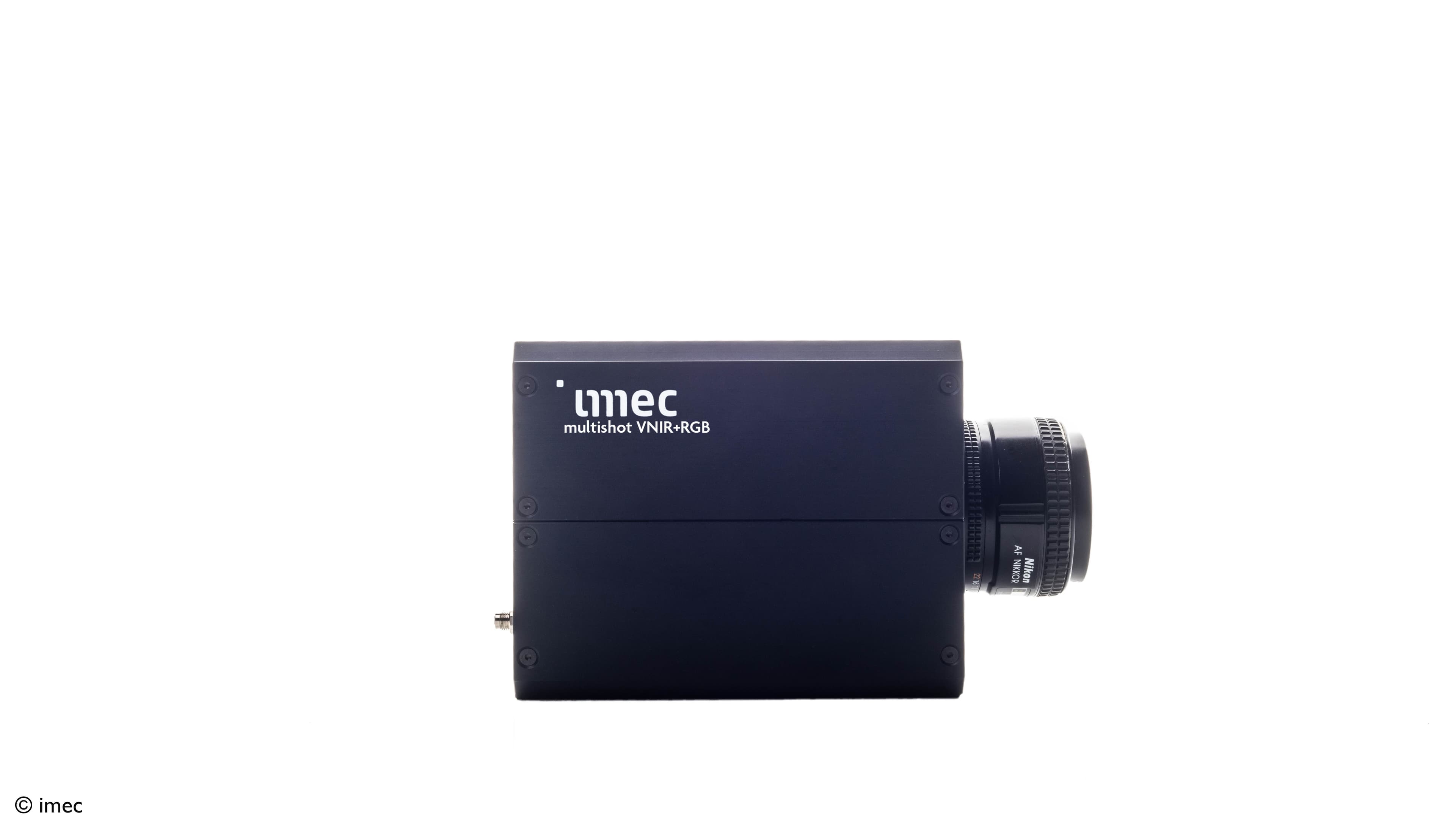
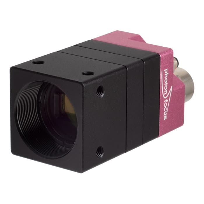
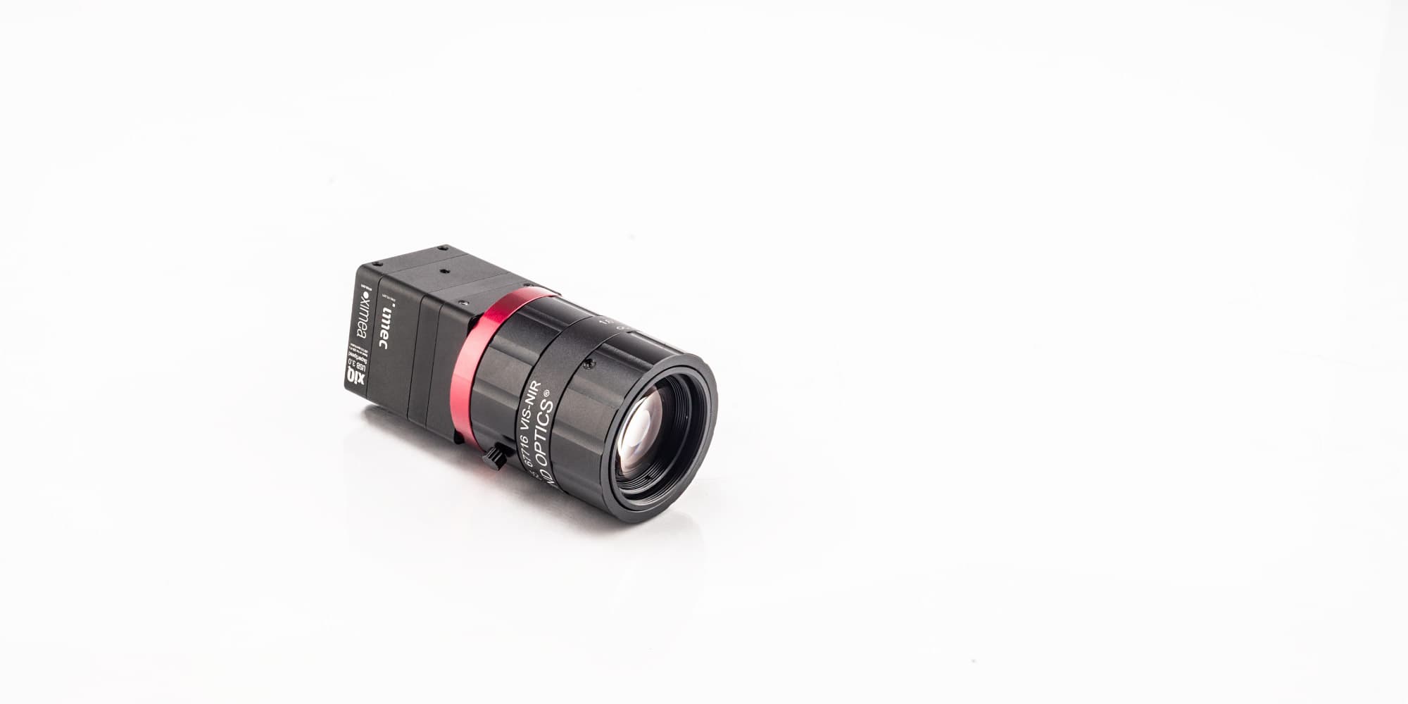
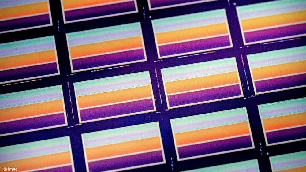
The new spectral detector enables hyperspectral imaging from a compact camera of the same size as a regular RGB camera. Due to its monolithically integrated on-chip spectral stack, there is no need for external alignment and integration of filters, since the filter stack is an integral part of the image sensor chip.
The optimised design has 10 detector lines per spectral band, double that of its predecessor, the LS150, and a signal-to-noise ratio that is 40% higher than that of the LS150.
The new detector is now also equipped with a set of black zones in between the stacks of spectral filters to allow a more accurate noise and dark current correction – determined under the exact same conditions (like sensor temperature) as the image acquisition.
Precision engineering meets high-volume manufacturability
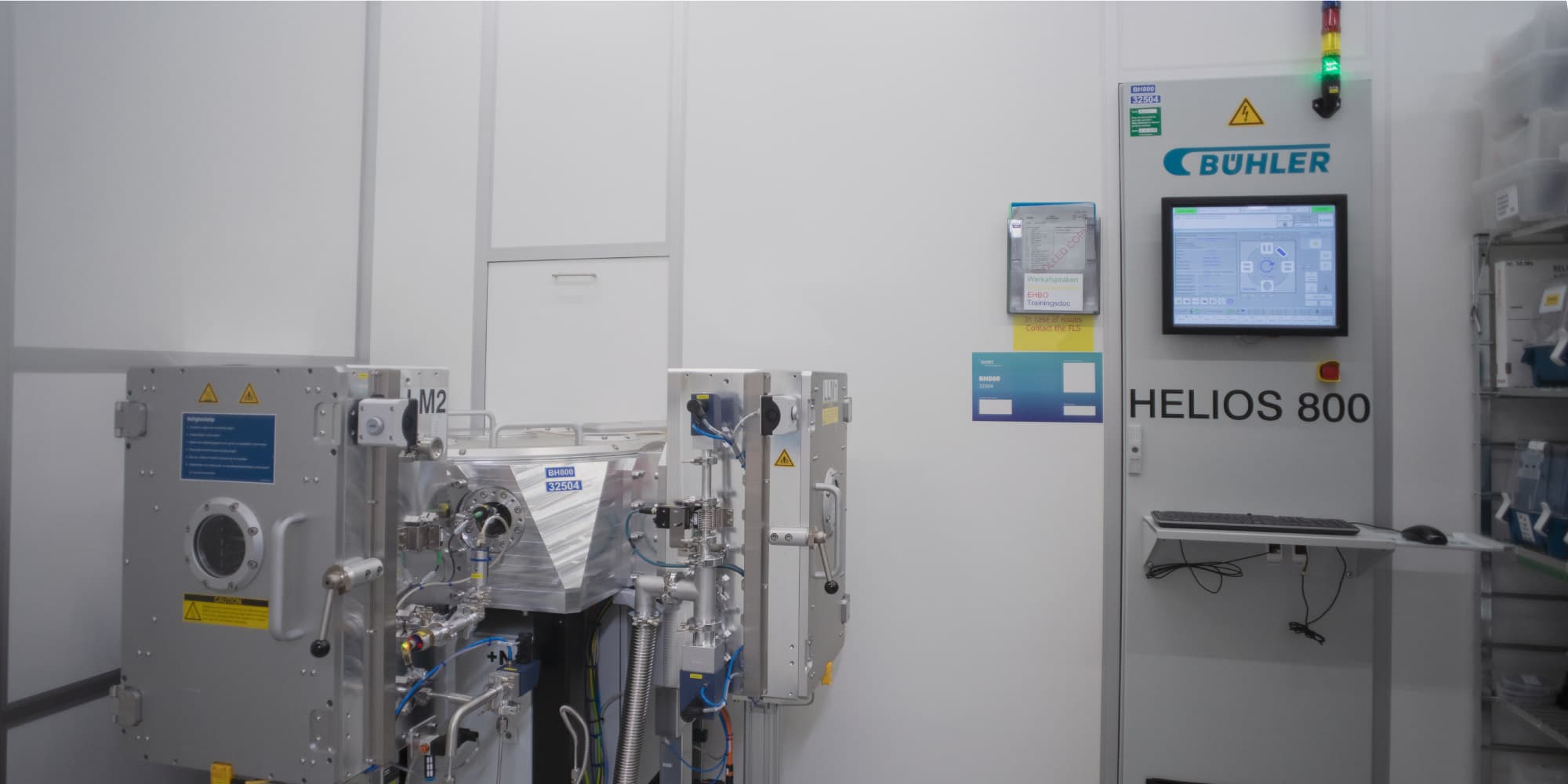
A primary focus was ensuring high-throughput manufacturability without sacrificing the precision required for e.g. high-end applications. To achieve this, imec optimized the process technology using its infrastructure supporting both 200mm and 300mm wafers. Part of this is a customized optical deposition tool developed in collaboration with Bühler Group.
All this enables the high-precision, monolithically integrated filter-on-chip CMOS sensors to be produced with unmatched consistency (i.e. low variability between the different sensors, giving the advantage that you can more consistently do measurements with the same sensors).
The resulting optimized fabrication process ensures low sensor-to-sensor variability – the central wavelength variability has been reduced down to 1%, which is a 5x improvement in comparison to the devices manufactured with the previous tools.
This is critical for companies deploying high-end applications where uniform data across multiple units is essential for accurate analysis. Just think of advanced medical application, industrial vision, Earth observation, or precision agriculture applications where consistent spectral signatures are vital.
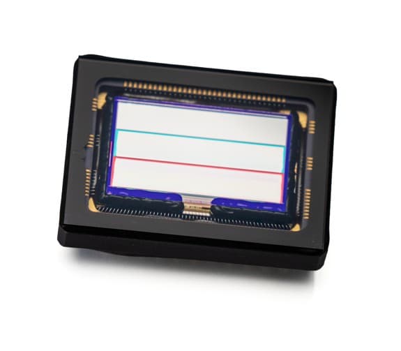
Imec LS96 linescan hyperspectral sensor with 96 bands.
Technical specifications and performance
The new sensor sets a new standard for light sensitivity and spectral range in a compact form factor. Key technical highlights include:
- Spectral range: 450–900 nm, divided equidistantly into 96 spectral bands.
- Enhanced sensitivity: features 10 detector lines per spectral band, enabling 10 digital TDI (time-delayed-integration) stages per band, to provide increased signal-to-noise ratio (SNR). As compared to its predecessor, the LS150, the number of detector lines is doubled and the SNR is improved by 40%.
- Resolution and speed: built on the flight-proven AMS CMV2000 sensor, it offers a resolution of 2048px with a 2/3” optical format and frame rates up to 340fps at full resolution.
- Operational flexibility: users can define multiple regions of interest (ROI), allowing the sensor to operate at full spectral resolution or focus on specific bands to reduce data load and further increase frame rates.
Robust design for harsh environments
By monolithically integrating specialized thin-film spectral filters directly onto the CMOS detector, imec has created a configuration that is inherently robust and stable.
Unlike traditional optical setups that use separate elements, such as prisms or gratings, this integrated design guarantees exceptional filter-to-detector alignment and is highly resistant to the shocks and vibrations encountered during e.g. satellite launch or drone flight for precision agriculture or PV inspection analysis.
Ready for integration
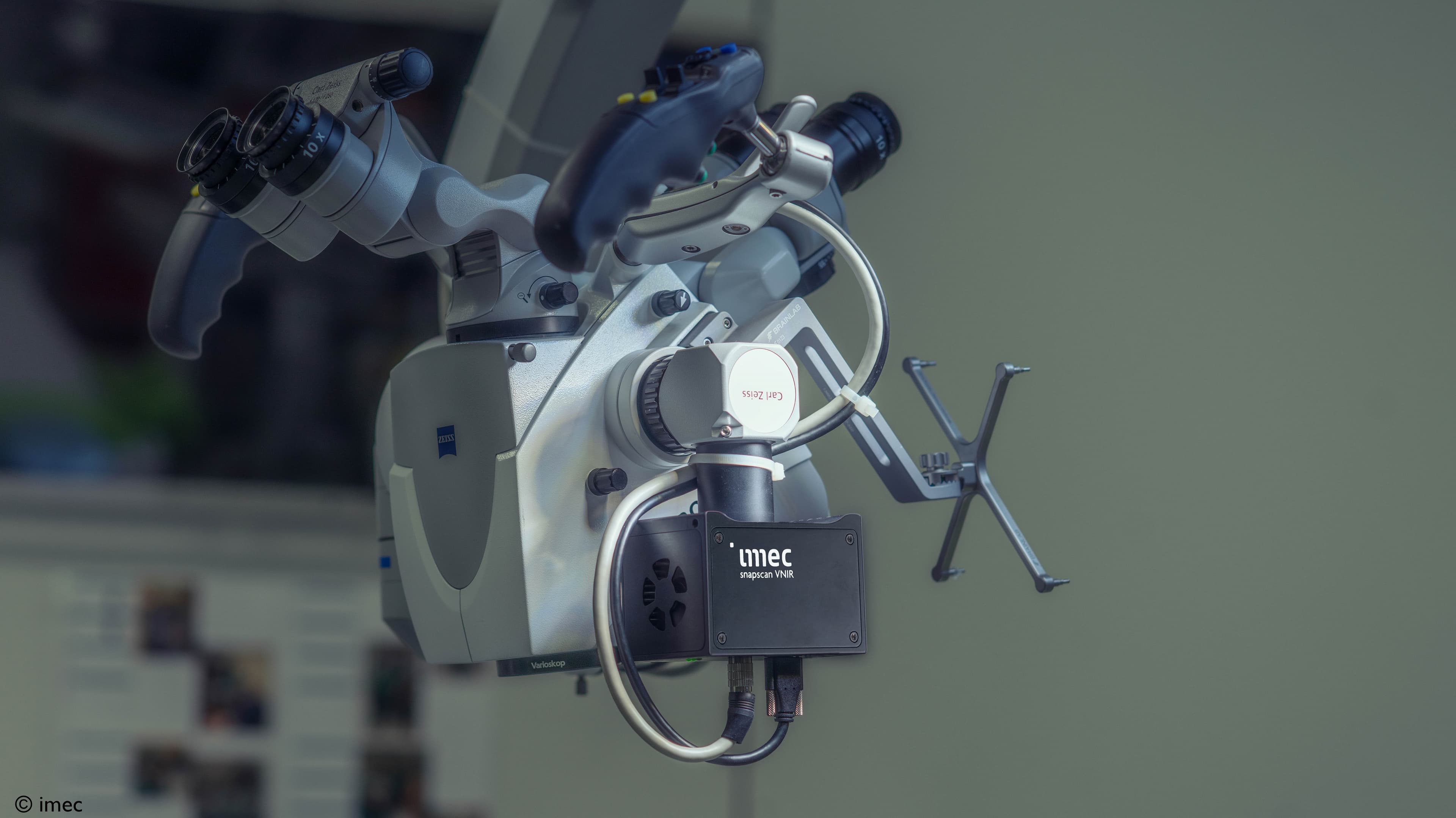
This sensor is designed to meet the growing demand for high-quality data in Earth observation missions, along with industrial and medical applications. It is now available to camera developers, system integrators and research partners for evaluation and integration into next-generation spectral imaging systems, providing low-barrier access to imec's cutting-edge spectral imaging-on-chip technology.
The compact form factor coupled with a combination of excellent sensitivity, uniformity, resolution and speed enables applications such as conveyor belt-based industrial inspection (automated waste sorting & recycling, food inspection, quality control), and drone-based remote monitoring (precision agriculture – e.g. yield optimization, soil mapping, disease detection; PV installation inspection; oceanography – e.g. coast erosion).
Furthermore, following fast in-field learning cycles with this sensor, customized filter stacks can be also implemented on other sensor types to realize specific architectures based on dedicated use case specifications.
For technical inquiries and purchasing information, contact hsi.sales@imec.be or book a meeting during VISION from October 6 till 8, 2026 in Stuttgart. Hope to see you!