This article was published previously in EETimes.
Semiconductor industry leading the way in PFAS reduction
Per- and polyfluoroalkyl substances (PFAS) have been a cornerstone in various industries due to their unique properties, including resistance to heat, water, and oil. However, the persistence of these ‘forever chemicals’ in the environment and potential health risks have led to increasing regulatory scrutiny and a push towards finding alternatives. The semiconductor industry, which relies on PFAS for their unique properties in processes like lithography and etching, is now at the forefront of this transition. Despite growing efforts to reduce PFAS use, semiconductor lithography still relies on these materials.
As a leading research institute at the heart of the semiconductor ecosystem, imec is ideally positioned to take the lead in addressing this challenge. With strong partnerships across the supply chain –including device manufacturers, material suppliers, and equipment makers– imec plays a crucial role in driving the industry's transition toward PFAS-free manufacturing. By leveraging its central position and deep expertise, imec actively supports the development, verification, and eventual implementation of sustainable alternatives.
This article delves into the efforts and challenges faced by the semiconductor industry, particularly through the lens of imec's initiatives, to eliminate PFAS from their materials
Collaboration drives imec’s progress toward PFAS-Free lithography materials
Imec’s collaboration with its partners has been pivotal in the journey towards PFAS-free materials. This initiative began in the summer of 2023, following a push from key industry players to find PFAS-free alternatives for lithography materials. Initially focused on chemically amplified resists (CAR) for extreme ultraviolet (EUV) lithography, the scope soon expanded to include deep UV (DUV) lithography, as well as other materials such as rinses and underlayers. To assess feasibility, imec engaged material suppliers, starting with a low-profile approach aimed at shortening PFAS chains. Encouraging early results led to a more ambitious target: achieving PFAS-zero materials, with the first phase centered on PFAS-free CAR for EUV lithography.
Sources of PFAS in CAR
In CAR, PFAS-containing compounds are primarily found in the photoacid generator (PAG), a key component that drives the resist’s chemical reaction. Fluorinated groups in PAGs help control acid diffusion, improve film uniformity, and lower surface energy, ensuring smooth coating and high-resolution patterning. Additionally, certain polymers in the resist formulation may contain PFAS in the form of fluorinated functional groups, such as trifluoromethyl (-CF₃), which contribute to solubility control and chemical stability. Beyond the polymer and PAG, other resist components may also introduce PFAS, depending on the formulation. For example, photo-decomposable quenchers (PDQs), which regulate acid diffusion and reaction kinetics, may contain varying levels of PFAS.
The exact composition of CAR varies between suppliers, as formulations are often proprietary and optimized for specific lithographic processes. While the core components –polymers, PAGs, and PDQs– are common across most CAR systems, their precise chemical makeup, including the presence and concentration of PFAS, can differ significantly. Some formulations may rely heavily on fluorinated polymers or PAGs with PFAS-based anions to enhance performance, while others may use alternative chemistries to achieve similar effects.
A rating system to compare PFAS-content across formulations
This variability makes it challenging to benchmark PFAS content across materials, as proprietary formulations are often undisclosed by suppliers. Without a standardized method for quantification, there is no clear metric to drive reduction efforts. To address this, imec developed a rating system that allows for a consistent calculation of PFAS content in photoresists. While imec’s PFAS rating system is still evolving, it is widely accepted by suppliers as a neutral and non-revealing method of benchmarking materials.
Imec’s system is based on a structured calculation method that accounts for all PFAS-contributing components in a resist formulation, including the polymer, PAG, PDQ, and other additives. It serves two key purposes. First, it enables a clear distinction between PFAS-free materials (rated as PFAS-zero or PFAS-free) and those containing PFAS at varying levels. Second, it provides IC manufacturers with a standardized way to request PFAS content information from suppliers without exposing proprietary details. The rating system was introduced in April 2024, and discussions are ongoing to refine and expand its scope to include other semiconductor materials.
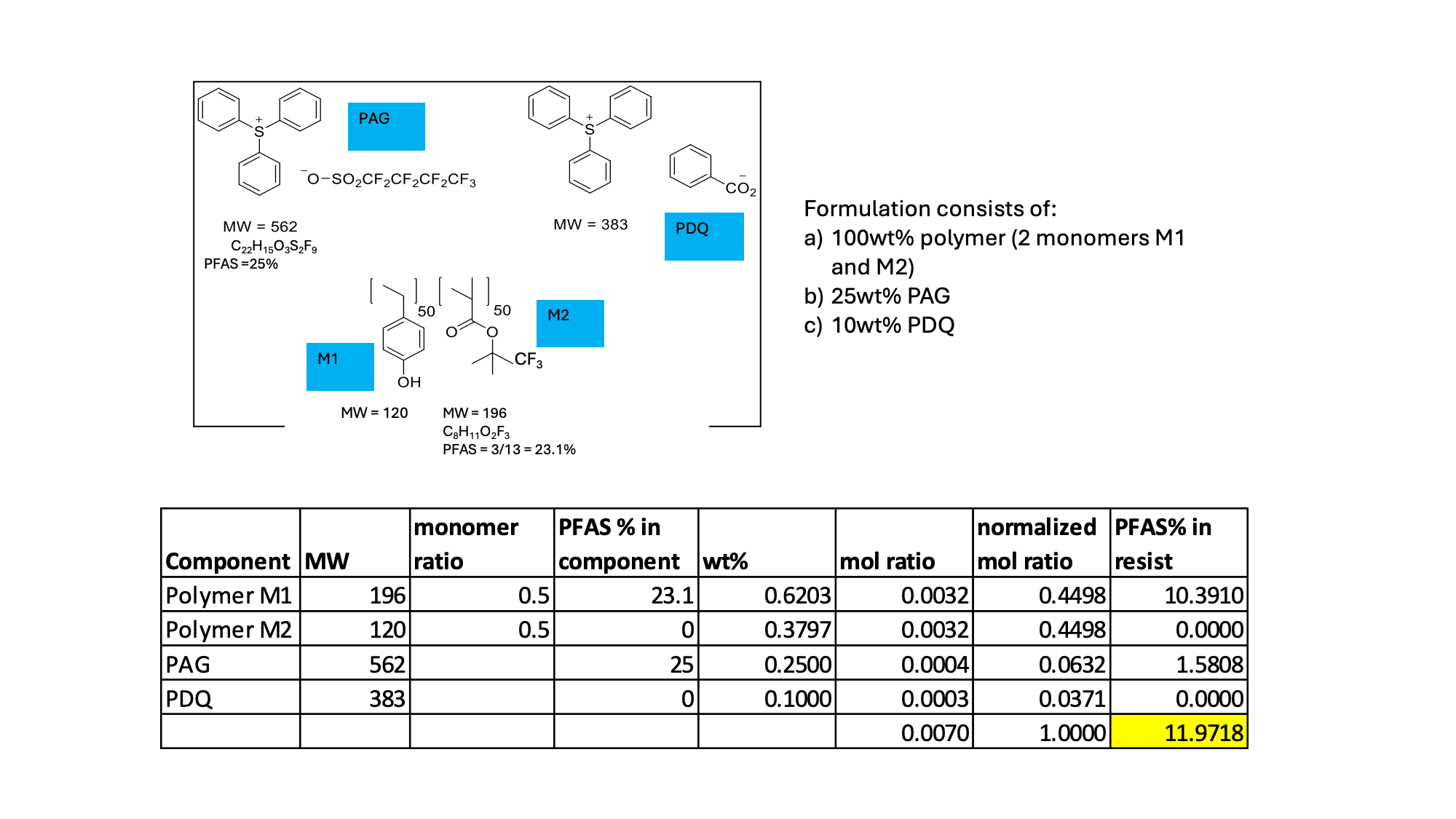
Fig 1 – Example of the rating system. The calculation follows a step-by-step approach: first, the molecular weight and monomer ratios of each component are determined. Then, the weight percentage of each compound in the resist formulation is factored in. Finally, the atomic percentage of PFAS within each component is calculated, explicitly excluding hydrogen atoms. To ensure consistency, aromatic fluorine structures are not considered PFAS, and solvents are omitted since they evaporate during processing.
PFAS-free and PFAS-containing resists show a comparable performance
A key factor in evaluating PFAS-free resists is how well they perform compared to traditional PFAS-containing materials in creating high-resolution patterns. Two critical structures were tested: dense line-space patterns at 32nm pitch and hexagonal contact holes at 36nm pitch. These patterns are fundamental to semiconductor manufacturing, as they directly impact the precision and reliability of chip features.
A notable finding was that the failure-free latitude (FFL)—a measure of how stable a resist is under process variations—was in some PFAS-zero cases as good as, or even better than, that of the PFAS-containing reference. This is significant because a larger FFL means greater process flexibility, reducing the risk of defects and improving overall manufacturability. Similarly, for contact holes, PFAS-free formulations produced well-defined, uniform features, with good circularity and critical dimension uniformity. This suggests that PFAS-free resists can maintain pattern fidelity under real-world conditions, an essential factor for ensuring electrical connectivity in advanced chips.
However, while these materials show strong potential, challenges remain in pushing resolution further. PFAS plays a critical role in resist chemistry, affecting acid diffusion, film uniformity, and overall process stability. Without it, resist formulations have fewer material options, making it harder to optimize for higher resolutions. Some trade-offs were also observed in terms of exposure latitude and defect control, highlighting areas that require further refinement.
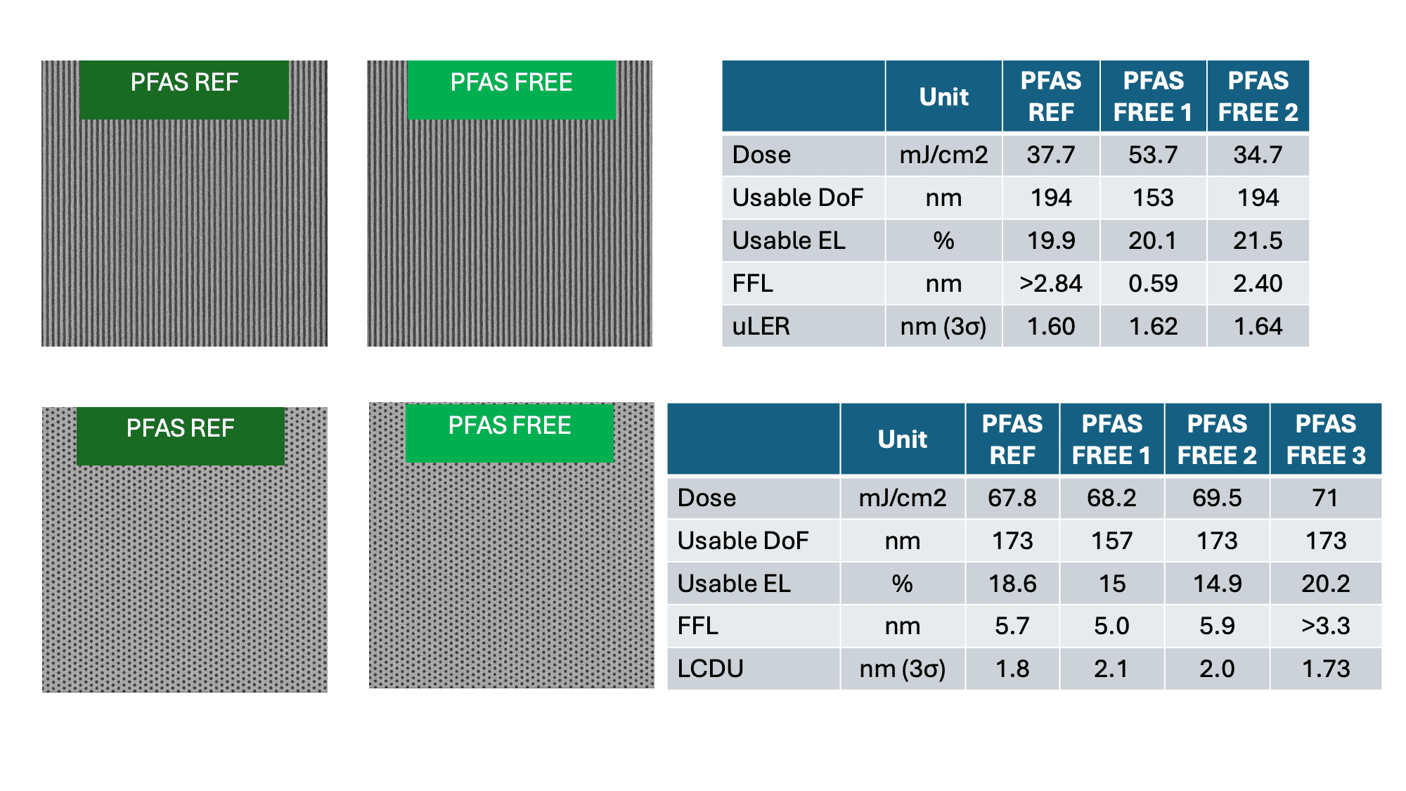
Fig 2 - Initial results of patterning with PFAS-free resists for 32nm pitch line space patterns (top) and 36nm pitch hexagonal contact holes (bottom) under optimal exposure conditions.
PFAS in semiconductor manufacturing
Beyond resists, PFAS appears in various stages of the lithographic material flow, including rinse materials, underlayers, and waste streams. They are used across semiconductor photolithography, including in bottom and top antireflective coatings (TARCs), anti-collapse rinses, and immersion top coatings. Their unique properties—such as high acidity, low refractive index, and strong barrier characteristics—are essential for resolution enhancement, dissolution control, and preventing pattern collapse. Each of these components requires a different approach—some, like anti-collapse rinses, can be replaced with PFAS-free alternatives, while others, such as TARCs and immersion top coatings, demand entirely new strategies for mitigation or removal.
One key area of progress is rinse materials, which, like resists, are being reformulated to eliminate PFAS. In recent tests, two PFAS-free rinse materials were evaluated during the development step of a positive tone PFAS-free CAR on a 32nm pitch dense LS pattern. One of the PFAS-free rinse materials showed comparable performance to the PFAS-based reference rinse, meeting key specifications for critical dimension (CD) control, line-edge roughness, and defectivity. The second alternative, however, exhibited random line collapse at target CD, highlighting the challenges in identifying stable replacements. Work is ongoing to further optimize these materials and ensure process stability.
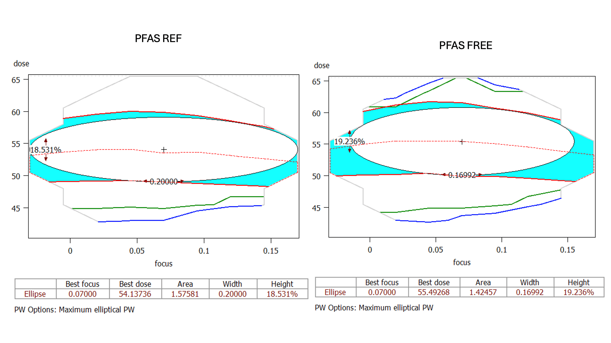
Fig 3 -Pitch 32nm dense LS patterning performance with the best PFAS-free positive tone resist tested with three different processes at the rinse step. The PFAS-free rinse that provided a comparable performance with respect to the rinse reference process is shown.
Evaluating Alternatives: MOR for EUV and PFAS-Free Solutions for DUV lithography
Within semiconductor manufacturing, the focus has been on PFAS-free CARs, given that CAR is the mainstream material used in lithography today. However, Metal-Oxide Resists (MORs) have emerged as a promising alternative, particularly for EUV applications. MORs, such as tin metal oxides, offer excellent resolution and etch resistance, making them attractive for the most aggressive pitches. Additionally, current MOR formulations are PFAS free.
Despite their advantages, MOR adoption is not yet widespread. One key reason is that MORs are primarily designed for EUV and extreme resolution applications, while CARs are still the standard for most semiconductor layers, including more relaxed pitches used in backend processing. As such, while MORs hold great potential for high-resolution applications, PFAS-free CAR remains the priority for broader implementation across multiple device layers.
The same is true for lithography technologies. While EUV represents the cutting edge of patterning, DUV immersion lithography remains widely used in semiconductor manufacturing, particularly for mature nodes and certain critical layers. However, removing PFAS from DUV lithography is even more challenging because DUV immersion relies on PFAS-based additives to prevent water-induced resist degradation and maintain pattern fidelity. In the past, this was managed using topcoats that acted as a barrier between the resist and the water, but today, many formulations integrate PFAS directly into the resist to achieve the same effect. Finding PFAS-free alternatives that provide the same level of process stability remains, therefore, a critical challenge. Imec is actively working with suppliers to develop solutions that balance environmental concerns with industry requirements.
A Comprehensive Approach to PFAS Elimination
Substitution alone is not enough—PFAS also persists in waste streams, requiring solutions for detection and removal. Current efforts focus on metrology techniques to measure PFAS levels in wastewater and process drains, ensuring an accurate understanding of the baseline contamination and types of PFAS present. This is an essential step in defining the long-term strategies for measuring, reducing and containing PFAS that are needed in fabs as replacement options are explored to eliminate PFAS. Current PFAS metrology is performed in labs, but in-line sensor development work has started. Even with better monitoring, PFAS remains difficult to break down. Abatement technologies are being explored to find effective ways to destroy PFAS molecules, preventing accumulation in the environment.
Eliminating PFAS from semiconductor manufacturing requires a holistic approach, addressing not just photoresists but all process steps where PFAS play a role. While significant progress has been made in developing PFAS-free CAR resists for EUV lithography, achieving full removal will require continued efforts across multiple areas, including rinses, underlayers, topcoats, and immersion additives. Beyond material development, successful adoption depends on thorough verification, seamless integration into existing processes, and scaling up for high-volume manufacturing.
As part of this transition, imec is working with partners across the semiconductor ecosystem to evaluate PFAS-free alternatives, optimize process conditions, and support the adoption of sustainable materials. Continued collaboration between material suppliers and device manufacturers will be essential to ensuring that environmentally friendly lithographic chemicals meet both performance and production demands. While challenges remain, ongoing research and industry-wide efforts will be critical in driving the shift toward PFAS-free semiconductor manufacturing.
Want to know more?
- The results were presented at the 2025 SPIE Advanced Litho + Patterning conference. More information can be found in the conference proceedings: D. De Simone, E. Gallagher. “Patterning performance of perfluoroalkyl substances (PFAS) free EUV chemically amplified resists: a step towards environmentally friendly lithographic chemicals,” in: 2025 SPIE Advanced Litho + Patterning Conference Proceedings.
- Read more about imec’s sustainability efforts, including eliminating PFAS from IC manufacturing in this article.