Towards useful quantum computers: better qubits, more qubits
Using quantum states for processing information has the potential to swiftly address complex problems that are beyond the reach of classical computers. Over the past decades, tremendous progress has been made in developing the critical building blocks underlying quantum computing technology.
In its quest to develop useful quantum computers, the quantum community focuses on two basic pillars: developing ‘better’ qubits and enabling ‘more’ qubits. Both need to be simultaneously addressed to obtain useful quantum computing technology.
The main metrics for quantifying ‘better’ qubits are their long coherence time (reflecting their ability to store quantum information for a sufficient period, as a quantum memory) and the high qubit control fidelity (linked to the ‘errors’ in controlling the qubits: sufficiently low a priori control errors are a prerequisite for successfully performing a quantum error correction protocol).
The demand for ‘more’ qubits is driven by practical quantum computation algorithms, which require the number of (interconnected) physical qubits to be in the millions, and even beyond. Similarly, quantum error correction protocols only work when the errors are sufficiently low: otherwise, the error correction mechanism actually ‘increases’ the error, and the protocols diverge.
Of the various quantum computing platforms that are being investigated, one stands out: Si quantum dot spin qubit based architectures for quantum processors – the ‘heart’ of a future quantum computer. In these architectures, nanoscale electrodes define quantum dot structures that trap a single electron (or hole), its spin states encoding the qubit.
Si spin qubits with long coherence times and high-fidelity quantum gate operations have been repeatedly demonstrated in lab environments and are therefore a well-established technology with realistic prospects. In addition, the underlying technology is intimately linked with CMOS manufacturing technologies, offering the possibility of wafer-scale uniformity and yield – an important steppingstone towards realizing ‘more’ qubits.
A sub-class of Si spin qubits uses metal-oxide-semiconductor (MOS) quantum dots to confine the electrons, a structure that closely resembles a traditional MOS transistor. The small size of the Si MOS quantum dot structure (~100nm) offers an additional advantage to upscaling.
Low qubit charge noise: a critical requirement to scale up
In the race towards upscaling, Si spin qubit technology can potentially leverage advanced 300mm CMOS equipment and processes that are known for offering a high yield, high uniformity, high accuracy, high reproducibility and high-volume manufacturing – the result of more than 50 years of downselection and optimization. However, the processes developed for CMOS may a priori not be the most suitable for fabricating Si spin quantum dot structures.
Si spin qubits are extremely sensitive to noise coming from their environment. Charge noise, arising from the quantum dot gate stack and the direct qubit environment, is one of the most widely identified causes of reduced fidelity and coherence. Two-qubit ‘hero’ devices with low charge noise have been repeatedly demonstrated in the lab using academic-style techniques such as ‘lift off’ to pattern the quantum dot gate structures.
This technique is ‘gentle’ enough to preserve a good quality Si/SiO2 interface near the quantum dot qubits. But this well-controlled fabrication technique cannot offer the required large-scale uniformity needed for large scale systems with millions of qubits. Industrial fabrication techniques like subtractive etch in plasma chambers filled with charged ions, or lithography-based patterning based on such etching processes, on the other hand, easily degrade the device and interface quality, enhancing the charge noise of Si/SiO2-based quantum dot structures.
First steps in the lab-to-fab transition: low charge noise and high-fidelity qubit operations achieved on an optimized 300mm CMOS platform
Imec’s journey towards upscaling Si spin qubit devices began about seven years ago, with the aim of developing a customized 300mm platform for Si quantum dot structures. Seminal work led to a publication in npj Quantum Information in 2024, highlighting the maturity of imec’s 300mm fab-based qubit processes towards large-scale quantum computers [1].
Through careful optimization and engineering of the Si/SiO2-based MOS gate stack with a poly-Si gate, charge noise levels of 0.6µeV/√Hz (at 1Hz) were demonstrated, the lowest values achieved on a fab-compatible platform at the time of publication. The values could be demonstrated repeatedly and reproducibly.

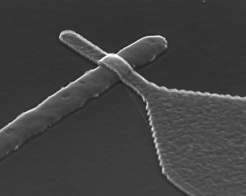
Figure 1 - Si MOS quantum dot structures fabricated using imec’s optimized 300mm fab-compatible integration flow.
More recently, in partnership with the quantum computing company Diraq, the potential of imec's 300mm platform was further validated [2]. The collaborative work, published in Nature, showed high-fidelity control of all elementary qubit operations in imec’s Si quantum dot spin qubit devices. Fidelities above 99.9% were reproducibly achieved for qubit preparation and measurement operations. Fidelity values systematically exceeding 99% were shown for one- and two-qubit gate operations, which are the operations performed on the qubits to control their state and entangle them.
These values are not arbitrarily chosen: in fact, whether quantum error correction ‘converges’ (net error reduction) or ‘diverges’ (the net error introduced by the quantum error correction machinery increases) is crucially dependent on a so-called threshold value, of about 99%: hence, fidelity values over 99% in fidelity are required for large-scale quantum computers to work.

Figure 2 – Schematic of a Diraq two-qubit device on a 300mm wafer, showing the full wafer, single die and single device level [2].
Charge noise was also measured to be very low, in line with the previous results from the npj Quantum Information paper [1]. Gate set tomography (GST) measurements shed light on the residual errors: with the low charge noise values, the coupling between the qubit and the few remaining residual nuclear-spin-carrying Si isotopes (29Si) turned out to be the main factor in limiting the fidelity for these devices. These insights show that even higher fidelities can be achieved through further isotopic enrichment of the Si layer with 28Si.
In the above studies, the 300mm processes were optimized for spin qubit devices in an overlapping gate device architecture. Following this scheme, three layers of gates are patterned in an overlapping and more or less self-aligned configuration to isolate and confine an electron. This multilayer gate architecture, extensively studied and optimized within the quantum community, offers a useful vehicle to study individual qubit metrics and small-scale arrays.
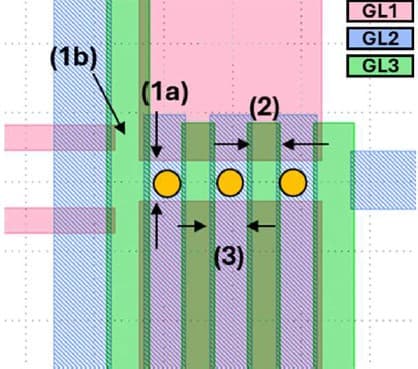
Figure 3 – Illustration of a triple quantum dot design using overlapping gates. Electrons are shown by the yellow dots. The gates reside in three different layers: GL1, GL2, and GL3 [3] (as presented at IEDM 2025).
The next step in upscaling: using EUV for gate patterning to provide higher yield, process control, and overlay accuracy
Thus far, imec used a wafer-scale, 300mm state-of-the art e-beam writer to print the three gate layers that are central to the overlapping gate architecture. Although this 300mm-compatible technique allows for great design flexibility and small pitches between quantum dots, it comes with a downside: its slow writing time does not allow printing full 300mm wafers in a reasonable process time.
At IEDM 2025, imec for the first time demonstrates the use of single-print 0.33NA EUV lithography to pattern the three gate layers of the overlapping gate architecture [3]. EUV lithography has by now become the mainstay for industrial CMOS fabrication of advanced (classical) technology nodes; imec’s work demonstrates that it can be equally used to define and fabricate good quantum dot qubits.
This means a significant leap forward in upscaling Si spin qubit technology. Full 300mm wafers can now be printed with high yield and process control – thereby fully exploiting the reproducibility of the high-quality qubits shown in previous works. EUV lithography brings an additional advantage: it allows the different gates to be printed with higher overlay accuracy than with the e-beam tools, which benefits the quality of the qubits and allows being more aggressive in the dot-to-dot pitches.
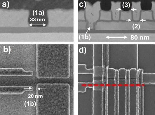
Figure 4 – TEM and SEM images after patterning the gate layers with EUV, highlighting critical dimensions [3] (as presented at IEDM 2025).
The imec researchers demonstrated excellent reproducibility, full-wafer room temperature functionality, and good quantum dot and qubit metrics at 10mK. Charge noise values were also comparable to measurements on similar ‘ebeam-lithography’ devices.
Inflection point: moving to scalable quantum dot arrays to address the wiring bottleneck
The overlapping gate architecture, however, is not scalable to the large quantum dot arrays that will be needed to build a quantum processor. The main bottleneck is in the connectivity: each qubit needs individual control and readout wiring, making the interconnect requirements very different from those of classical electronic circuits. In the case of overlapping gates, wiring fanout is provided by the different gate layers, and this imposes serious limitations on the number of qubits the system can have.
Several years ago, a research group at HRL Laboratories in the US came up with a more scalable approach to gate integration: the single-layer gate device architecture [4]. In this architecture, the gates that are needed to isolate the electrons (the so-called barrier and plunger gates) are fabricated in one and the same layer, more closely resembling how classical CMOS transistors are built and interconnected using a multilayer BEOL.
Today, research groups worldwide are investigating how large quantum dot arrays can be implemented in such a single-layer gate architecture, while ensuring that each qubit can be accessed by external circuits. At first sight, the most obvious way is a 2D lattice, similar to integrating large memory arrays in classic CMOS systems. But eventually, this approach will hit a wiring scaling wall as well. The NxN quantum dot array requires a large number of BEOL layers for interconnecting the quantum dots. Additionally, ensuring good access for reading and controlling qubits that are farther away from the peripheral charge sensors becomes challenging.
A trilinear quantum dot architecture: an imec approach
At IEDM 2021, imec therefore proposed an alternative, smart way of interconnecting neighboring silicon qubits: the bilinear array [5]. The design is based on topologically mapping a 2D square lattice to form a bilinear design, where alternating rows of the lattice are shifted into two rows (or 1D arrays). While the odd rows of the 2D lattice are placed into an upper 1D array, the even rows are moved to a lower 1D array. In this configuration, all qubits remain addressable while maintaining the target connectivity of four in the equivalent 2D square lattice array. These arrays are conceptually scalable as they can further grow in one dimension, along the rows.
Recently, the imec researchers expanded this idea towards a trilinear quantum dot device architecture that is compatible with the single-layer gate integration approach. With this trilinear architecture, a third linear array of (empty) quantum dots is introduced between the upper and lower rows. This extra layer of quantum dots now serves as a shuttling array, enabling qubit connectivity via the principle of qubit shuttling.

Figure 5 – The concept of mapping a 2D lattice onto a bilinear design and expanding that design to a trilinear architecture. In the illustration, the principle of qubit shuttling is illustrated for the interaction between qubits 6 and 12.

Figure 6 – Top view of a 3x5 trilinear single gate array, with plunger (P) and barrier (B) gates made in a single layer [3] (as presented at IEDM 2025).
The video below nicely explains how that works. In the trilinear array, single- and some of the two-qubit interactions can happen directly between nearest neighbors, the same way as in the bilinear architecture. For others, two-qubit interactions can be performed through the ‘shuttle bus’ that is composed of empty quantum dots. Take a non-nearest neighbor interaction between two qubits as an example. The first qubit is moved to the middle array, shuttled along this array to the desired site to perform the two-qubit operation with a second, target qubit, and shuttled back. These ‘all-to-all’ qubit interactions were not possible using the bilinear approach. Note that these interactions can only be reliably performed with high-fidelity quantum operations, to ensure that no information is lost during the shuttling operation.
Imec movie showing the schematics, conceptual operation and manufacturing of the trilinear quantum dot architecture.
But how can this trilinear quantum dot architecture address the wiring bottleneck? The reason is the simplified BEOL structure: only two metal layers are needed to interconnect all the quantum dots. For the upper and lower 1D arrays, barrier and plunger gates can connect to one and the same metal layer (M1); the middle ‘shuttle’ array can partly connect to the same M1 layer, partly to a second metal layer (M2). Alongside the linear array, charge sensors can be integrated to measure the state of the quantum dots for qubit readout.
The architecture is also scalable in terms of number of qubits, as the array can further grow along the rows. If that approach at some point hits a scaling wall, it can potentially be expanded to four, five or even more linear arrays – ‘simply’ by adding more BEOL layers.
Using EUV lithography to process the trilinear quantum dot architecture: a world first
At IEDM 2025, imec showed the feasibility of using EUV lithography for patterning the critical layers of this trilinear quantum dot architecture [3]. Single-print 0.33NA EUV lithography was used to print the single-layer gate, the gate contacts and the two BEOL metal layers and vias.
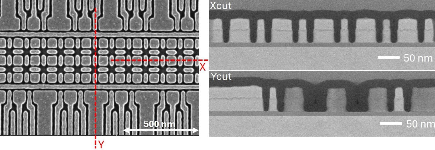
Figure 7 – Single-layer gate trilinear array after EUV lithography and gate etch with TEM cross sections in X and Y directions [3] (as presented at IEDM 2025).
One of the main challenges was achieving a very tight pitch across all the different layers, without pitch relaxation. The gate layer was patterned with a bidirectional gate pitch of 40nm. It was the first time ever that such an ‘unconventional’ gate structure was printed using EUV lithography – since most EUV lithography for classical CMOS applications focuses on unidirectional patterns. Next, 22nm contact holes were printed with <2.5nm (mean + 3sigma) contact-to-gate overlay in both directions. The two metal layers M1 and M2 were patterned with metal pitch in the order of 50nm.

Figure 8 – The trilinear array (a-c) after M1 and (d-f) after M2 patterning [3] (as presented at IEDM 2025).
In the race to upscaling, the use of EUV lithography allows full 300mm wafers to be processed with high yield, uniformity, and overlay accuracy between the critical structures. First measurements already revealed a room temperature yield of 90% across the wafer, and BEOL functionality was confirmed using dedicated test structures. The use of single-patterning EUV lithography additionally contributes to cost reduction (by avoiding complex multi-patterning schemes) and to the overall resolution of the printed features. Moreover, the complexity and asymmetry of the 2D structure cannot be achieved with double patterning techniques.
Conclusion and outlook: upscaling and further learnings
In pursuit of enabling quantum systems with increasingly more qubits, imec made major strides: (1) reproducibly achieving high-fidelity unit cells on two-qubit devices; (2) transitioning from ebeam to EUV lithography for patterning critical layers, and (3) moving from overlapping gate architectures to a single-layer gate configuration.
Adding EUV to imec’s 300mm fab-compatible Si spin qubit platform will enable printing high-quality quantum dot structures across a full 300mm wafer, with high yield, uniformity, and alignment accuracy.
The trilinear quantum dot architecture, compliant with the single-layer gate approach, will allow upscaling the number of qubits by addressing the wiring bottleneck. Currently, work is ongoing to electrically characterize the trilinear array, and to study the impact of both the single-layer gate approach and the use of EUV lithography on the qubit fidelities.
The trilinear quantum dot architecture is a stepping stone towards truly large-scale quantum processors based on silicon quantum dot qubits: it may eventually not be the most optimal architecture for quantum operations involving millions of qubits, and clear bottlenecks remain. But it is a step in the learning process towards scalability and allows de-risking the technology around it. It will enhance our understanding of large-scale qubit operations, qubit shuttling, and BEOL integration. And it will allow exploring the expandability of the architecture towards a larger number of arrays.
In parallel, imec will continue working on the overlapping gate structure which can offer very high qubit fidelities. These high-quality qubits can be used as a probe to further study and optimize the qubit’s gate stack, understand the limiting noise mechanisms, tweak and optimize the control modules, and develop the measurement capability for larger scale systems in a systematic, step-by-step approach – leveraging the process flexibility offered by imec’s 300mm infrastructure. It’s an outstanding research vehicle in the quest for better qubits, providing learnings much faster than any large-scale quantum dot architecture. It can help increase our fundamental knowledge of two-qubit systems, an area in which there is still much to learn.
This article was originally published in EDN.
Want to know more?
[1] ‘Low charge noise quantum dots with industrial CMOS manufacturing,’ A. Elsayed et al., npj Quantum Inf 10, 70 (2024). https://doi.org/10.1038/s41534-024-00864-3;
[2] ‘Industry-compatible silicon spin-qubit unit cells exceeding 99% fidelity,’ P. Steinacker et al., Nature 646, 81–87 (2025). https://doi.org/10.1038/s41586-025-09531-9;
[3] ‘300mm fabrication of silicon quantum dot spin qubits using 0.33NA EUV lithography;’ S. Beyne et al., IEDM 2025;
[4] ‘A flexible design platform for Si/SiGe exchange-only qubits with low disorder,’ Ha, Wonill et al., Nano Letters 22.3 (2021): 1443-1448;
[5] ‘Large-scale 2D spin-based quantum processor with a bi-linear architecture’, F.A. Mohiyaddin et al., IEDM 2021.