Exploration of Atomic Layer Etching to enable Metal-Assisted Transfer of 2D Transition Metal Dichalcogenides
Leuven | About a week ago
The global rise in electronic device and data centre use has sharply increased demand for faster, denser, and more energy-efficient semiconductors. Improvements now focus on miniaturization, new materials, and novel device physics. However, traditional silicon transistors struggle below 10 nm due to poor gate control and remote phonon scattering. While stacked silicon nanosheets offer higher current density, their ultra-thin channels are prone to roughness and short-channel effects.
Monolayer 2D materials are ideal materials for next-generation logic devices (e.g., complementary metal-oxide semiconductor (CMOS) transistors), photodetectors, sensors, and light-emitting diodes due to their excellent semiconductor and optical properties. Monolayer transition metal dichalcogenides (MX2), such as molybdenum disulfide (MoS2) and tungsten disulfide (WS2), with their intermediate bandgaps and intrinsic resistance to short-channel effects, provide better mobility and superior gate control than silicon at atomic thickness, thereby enabling further transistor downscaling. High-quality MX2 monolayers are obtained by epitaxial growth on templated substrates such as sapphire, and scalability to large substrates (300 mm) is ensured by metal-organic chemical vapor deposition (MOCVD). C-plane sapphire is highly effective in promoting epitaxial MX2 growth, owing to its lattice symmetry match, chemical inertness toward MOCVD precursors, and the capacity to precisely control surface reconstruction and roughness.
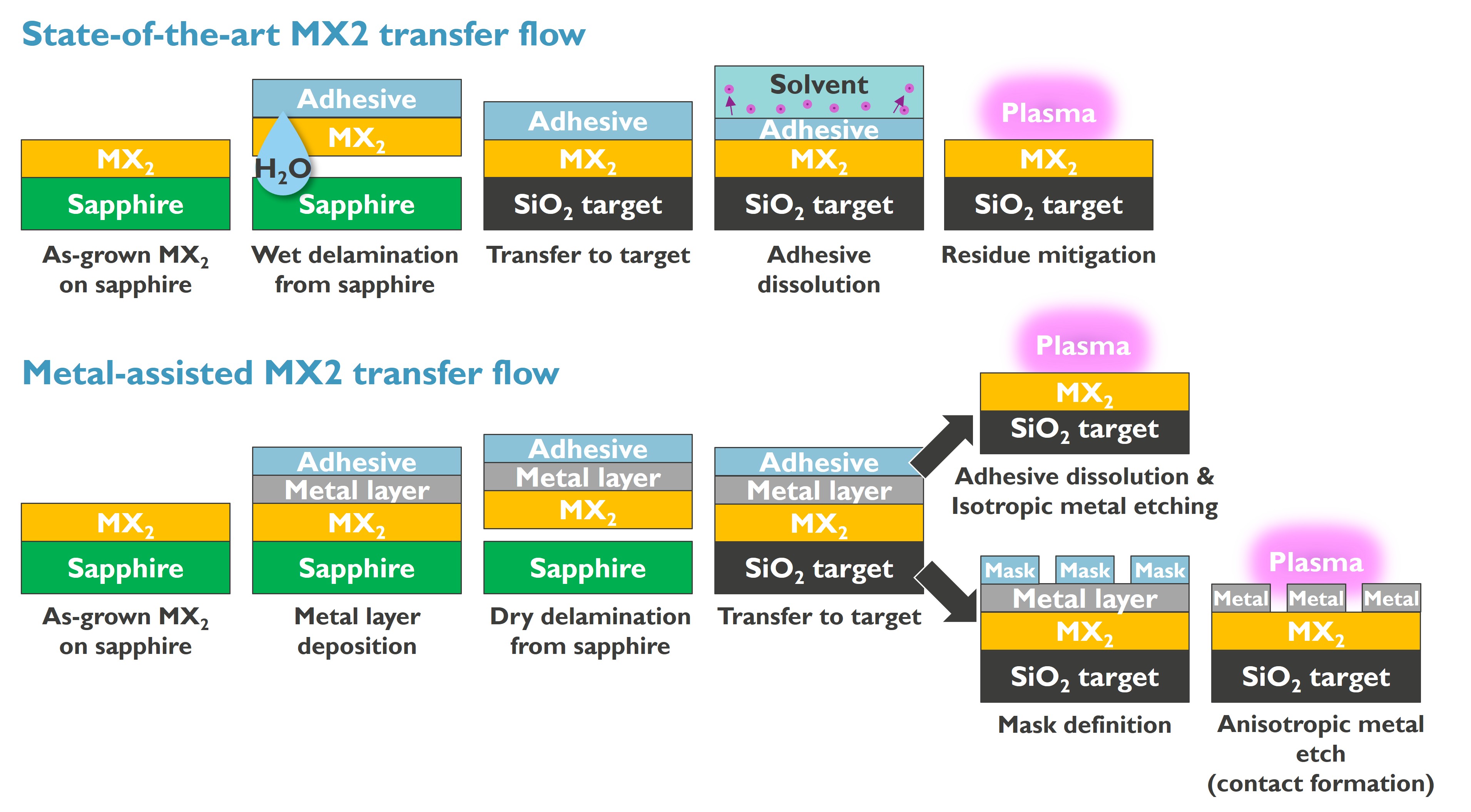
Despite its benefits for epitaxy, sapphire cannot be used for CMOS device fabrication. This necessitates a layer-transfer step, transferring the MX2 monolayer from the sapphire growth substrate to conventional silicon substrates for further CMOS fabrication. The development of layer-transfer technology is essential to enable the integration of MX2 in future nano-electronic devices. State-of-the-art transfer technologies (see fig.1, top, State-of-the-art MX2 transfer flow) rely on polymer adhesives that inherently make them susceptible to residue incorporation (carbon contamination), leading to significant deterioration of subthreshold swing (slower transistors) or unintentional doping.
Another major challenge in the integration of 2D materials lies in contact formation. Unlike in Si, the source-drain contacts for MX2 transistors are metals, where achieving ohmic contact formation and mitigating Fermi level pinning remain critical hurdles for CMOS integration. The contact resistance (Rc) is determined not only by the electronic properties of the metal-2D interface but also by damage to the 2D material induced during metal deposition. Certain metals can chemically react with the MX2, leading to unwanted alloying. The metal deposition itself may cause additional physical damage, including amorphization, sulfur depletion, strain, and phase transitions. Furthermore, carbon residues on top of the 2D material, originating from the transfer process, can significantly increase resistance.
In the metal-assisted transfer sequence, a (semi-)metal buffer layer is inserted between the adhesive and the MX2 (see Fig. 1 bottom, Metal-assisted MX2 transfer flow). This buffer prevents direct contact between the adhesive polymer and the 2D monolayer, enabling a clean, fully dry transfer process (no carbon residues). The same metal buffer layer can subsequently serve as a contact metal through selective patterning. The choice of buffer metal is guided by lattice cohesion energy, as low values favor low-damage nucleation and congruent deposition with the MX2 crystal lattice. Bismuth is a primary candidate; other options are Sb (antimony) and In (indium).
The proposed PhD work will focus on most critical step of the transfer process: metal recess and patterning selective to the MX2 monolayer. For this, the PhD research will employ novel etching strategies based on Atomic Layer Etching (ALE), with a primary focus on dry etching. The work will focus on exploring a variety of dry etch methods (plasma, vapor), covering both isotropic and anisotropic metal removal, for individual metals and binary alloys. Isotropic etching will be first investigated through Transient Assisted Plasma Etch (TAPE) employing H2-based downstream plasma with suitable additives to achieve high selectivity toward MX2. Anisotropic etching will be studied using pulsed Inductively Coupled Plasma (ICP) with passivating molecules to protect nanostructure sidewalls during patterning. The goal is to enable the advanced contact patterning for the fabrication of MX2 transistor devices on Si-substrates (channel length < 50 nm).
Required background: Master in chemistry, physics, engineering, nanosciences
Type of work: 60% experimental, 30% data analysis, 10% literature
Supervisor: Annelies Delabie
Daily advisor: Jean-Francois de Marneffe
The reference code for this position is 2026-177. Mention this reference code on your application form.