Low-noise amplifier based on GaSb for quantum computing
Leuven | More than two weeks ago
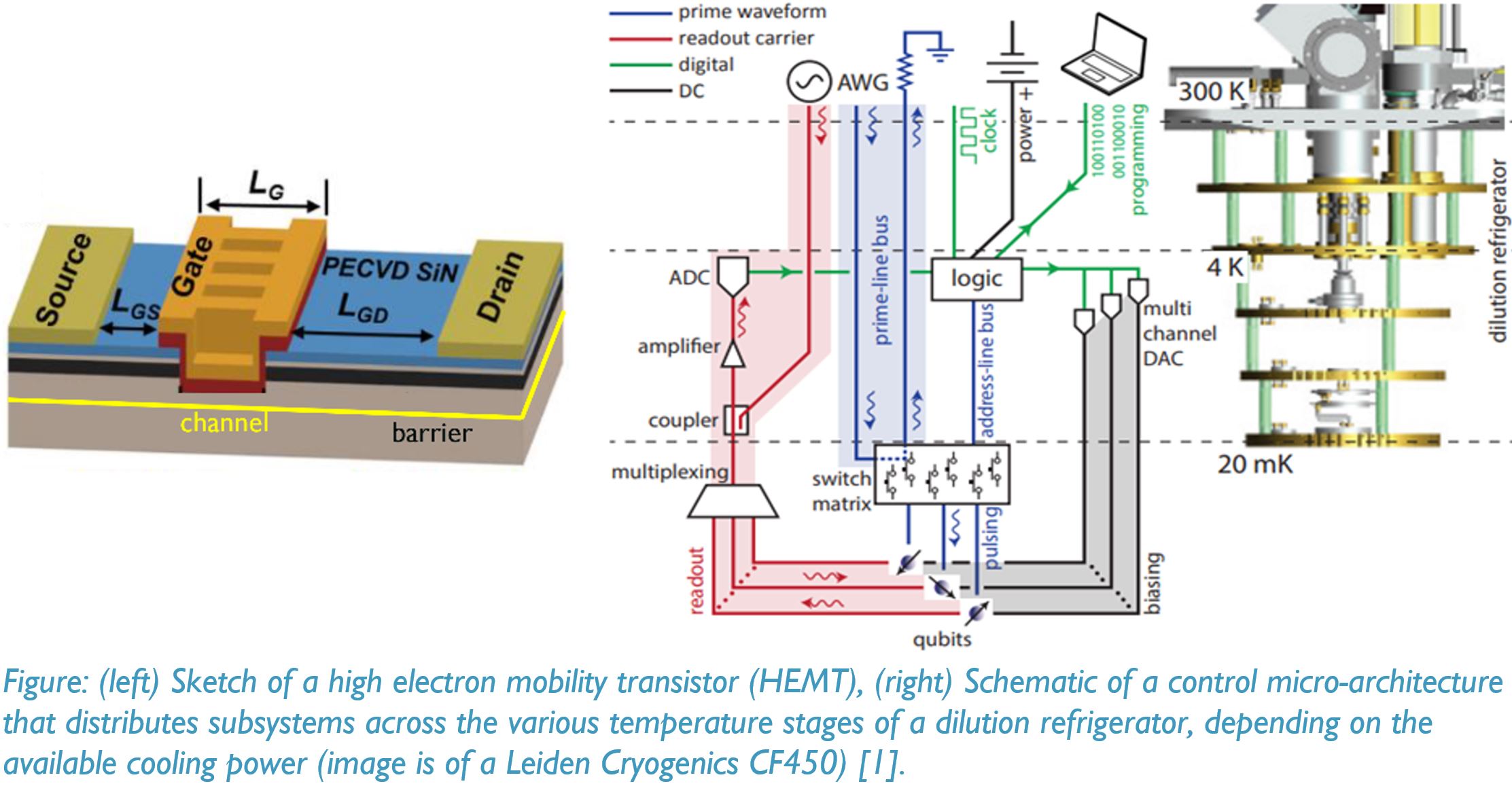
The read-out of qubits operating at cryogenic temperatures is a real challenge [1]. A key component in the amplification chain (right figure below) of the weak signals is a low-noise amplifier (LNA) with the highest possible signal-to-noise ratio and operating below 4K. An additional very crucial requirement for the LNA is low power dissipation due to the limited cooling power of cryostats. III-V high electron mobility transistors (HEMT, left figure below) are the superior technology meeting these requirements.
Nano-ridge engineering (NRE) [2] is a unique monolithic integration approach for III-V devices on Si substrates introduced by imec. This hetero-epitaxial concept is based on selective area growth by metal-organic vapor phase epitaxy (MOVPE). The monolithic integration starts with the III-V deposition inside deep narrow trenches, fabricated on a Si substrate. The growth in these high aspect ratio trenches ensures efficient trapping of misfit defects caused by lattice mismatch between III-V materials and Si which leads to improved III-V crystal quality. Once the trenches are filled, the crystal continues to grow outside of the trench where the nano-ridge shape and volume can be manipulated by the MOVPE growth conditions. NRE is successfully demonstrated for GaAs, GaSb and InGaAs [3][4]. Various devices such as heterojunction bipolar transistors [5], lasers [6] and photodetectors [7] were already demonstrated emphasizing the large potential of this approach.
The topic of this PhD project is the development of state-of-the-art NRE based hetero-structures exploring different antimony-based III-V alloys, e.g., GaAsSb, GaPSb, InPSb, as barrier layer for a InAs channel HEMT with a clear focus on low-noise, high speed and low operating power of the device.
During your PhD you will
- Design and execute growth experiments on MOVPE reactors and understand the physics/thermodynamics behind the deposition process
- Carry out device processing
- Master structural and electrical characterization techniques
- Acquire knowledge on defect formation in the grown 3D nano structures
- Interpret the analysis results of your device samples and relate your observation with device modelling
- Gain insight in the HEMT device physics and electrical characterization.
The epitaxial growth, device processing and characterization of your samples will be done at imec, Leuven.
[1] J.M. Hornibrook et al., “Cryogenic Control Architecture for Large-Scale Quantum Computing”, Phys. Rev. Applied, vol. 3, 024010, 2015.
[2] B. Kunert et al., “Gaining an edge with nano-ridges”, Compd. Semiconductor, vol. 24, no. 05, pp. 36–41, 2018.
[3] M. Baryshnikova et al., “Nano-Ridge Engineering of GaSb for the Integration of InAs/GaSb Heterostructures on 300 mm (001) Si”, Crystals, vol. 10, no. 4, p. 330, 2020.
[4] B. Kunert et al., “Application of an Sb Surfactant in InGaAs Nano-ridge Engineering on 300 mm Silicon Substrates”, Cryst. Growth Des., vol. 21, no. 3, pp. 1657–1665, 2021.
[5] A. Vais et al., “First demonstration of III-V HBTs on 300 mm Si substrates using nano-ridge engineering”, 2019 IEEE International Electron Devices Meeting (IEDM), 9.1.1-9.1.4, 2019.
[6] Y. Shi et al., “Loss-coupled DFB nano-ridge laser monolithically grown on a standard 300-mm Si wafer”, Opt. Express, vol. Part F140-, no. 10, pp. 14649–14657, 2019.
[7] C. I. Ozdemir et al., “Low Dark Current and High Responsivity 1020nm InGaAs/GaAs Nano-Ridge Waveguide Photodetector Monolithically Integrated on a 300-mm Si Wafer”, J. Light. Technol., vol. 39, no. 16, pp. 5263–5269, 2021.

Required background: Master’s degree in Physics, in material science and engineering, in chemical engineering or equivalent
Type of work: 30% sample growth, 30% structural and electrical characterization, 10% processing, 30% device modelling and literature research
Supervisor: Nadine Collaert
Co-supervisor: Bernardette Kunert
Daily advisor: Yves Mols
The reference code for this position is 2025-078. Mention this reference code on your application form.
