
The AI race is often framed as a race for bigger models, faster chips and larger data centers. That framing is outdated. The real bottleneck is scalability: moving, storing, cooling and powering intelligence as AI shifts from single models to agentic systems, and as it expands from today’s data centers to physical AI in a myriad of applications and form factors. That pushes us beyond a one-size-fits-all approach. The next compute multiplier will not come from one heroic invention by a single company, but from orchestrating logic, memory, fabric, architecture, algorithms and manufacturing into one coherent innovation system.
Inference becomes a memory and connectivity problem
In today’s agentic AI, intelligence no longer sits in one model answering one prompt. It emerges from chains of models, tools and agents that need to exchange context continuously. That means inference becomes a memory-and-connectivity challenge as much as a compute problem. The cost is no longer just in calculating answers, but in keeping data close enough, fast enough and energy-efficient enough to make reasoning practical at scale.
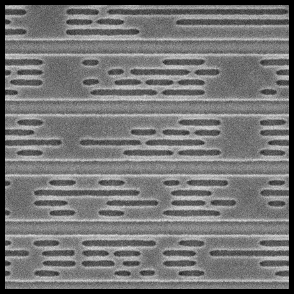
CMOS scaling will continue, with high-NA EUV soon pushing patterning deep into the angstrom era. But lithography alone will not meet AI’s demand for performance per watt and performance per area. The next Moore’s Law is becoming a system-level law: progress will come from multiplying gains across logic and memory scaling, fabric, architecture and algorithms.
As conventional electrical interconnects hit limits in bandwidth, energy efficiency and scalability, silicon photonics is starting to offer a path toward a more efficient fabric for AI workloads and the infrastructure behind them. The same is true for memory. For decades, compute and memory chips evolved largely independently, but agentic AI makes that separation untenable, because these systems increasingly depend on keeping context, parameters and agents close to the compute. Through advanced 2.5D and 3D integration, memory is literally becoming part of the system architecture rather than a separate component. Future performance gains will increasingly come from designing compute and memory together.
From a single roadmap to CMOS 2.0
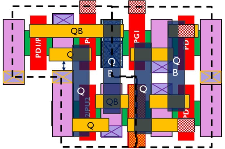
Without coordinated roadmaps across devices, integration and architectures, however, photonics and advanced packaging remain a collection of promising components rather than the fabric of scalable AI. What we call “CMOS 2.0” captures the shift toward a coordinated approach across the stack: moving from a single CMOS scaling roadmap to a richer design space of stacked logic layers, heterogeneous devices, advanced interconnects and ever-tighter compute-memory integration.
That richer design space also creates new and complicated optimization challenges. Power, thermal behavior, memory, packaging, software and reliability are becoming highly interdependent. This requires what we call cross-technology co-optimization (XTCO), a methodology for co-optimizing across technologies and physics as early in the design process as possible, so that improving one layer doesn’t weaken the system as a whole.
Orchestration as a competitive advantage
No single company can solve this puzzle alone. The bottlenecks now cut across foundries, fabless companies, IDMs, equipment suppliers, EDA vendors, hyperscalers, disruptive startups, universities and research organizations.
Ecosystem orchestration is therefore no longer a support function; it has become one of the semiconductor industry’s defining sources of competitive advantage. In practice, technology and ecosystem orchestration means shared roadmaps, early validation, test vehicles for XTCO and a shorter loop between research, design and manufacturing, ultimately bridging the gap from lab to fab.
In the AI era, the semiconductor ecosystem can no longer solve scalability alone, at least not in the form in which it has traditionally operated. That ecosystem has excelled at bringing together deep expertise across materials, devices, equipment, process technology and manufacturing to enable breakthroughs in manufacturability. But AI now forces a broader, more holistic optimization challenge: performance, energy efficiency and scalability have to be addressed across compute, memory, interconnects, packaging, software, algorithms and infrastructure. The collaboration model itself must expand, bringing foundries, IDMs, equipment suppliers and research organizations together with fabless companies, algorithm labs, hyperscalers and emerging neocloud players.
Ultimately, the winners of the AI race will be those that can extend the semiconductor industry’s proven model of ecosystem collaboration beyond manufacturability, connecting fabs, fabless innovators, algorithm labs and neoclouds into one coordinated effort to scale compute sustainably.
This article is published on Semiconductor Digest

Patrick Vandenameele is Chief Executive Officer at imec - a globally recognized R&D center specializing in nanoelectronics and digital technologies - since April 1, 2026. His leadership underpins imec’s commitment to addressing market-driven application challenges while advancing its world-class technology platforms through targeted internal investments and external collaborations.
Prior to this appointment as CEO, he served as Executive Vice President and Co-Chief Operating Officer at imec, where he was overseeing and shaping the organization's R&D strategy and its execution. In this position, Patrick was responsible for shaping and driving the center’s innovation agenda, ensuring the alignment of research initiatives with emerging market needs, partner priorities and technological frontiers. Previously, as chief portfolio officer at imec until early 2024, he spearheaded strategic initiatives spanning business development, portfolio management, and venture creation.
Holding a PhD from KU Leuven, Patrick began his journey with imec in 1996, contributing to the wireless communications program. In 2000, he transitioned to entrepreneurship, founding and leading several deep-tech ventures, three of which were built on imec technology. Patrick also held senior positions at top semiconductor firms like Qorvo and Hisilicon/Huawei, leading 11 product launches and overseeing over 100 million units shipped. After returning to imec in 2017, Patrick has been instrumental in expanding imec’s venture development activities, working closely with the deep-tech venturing fund imec.xpand to strengthen imec’s position as a pioneer in technology-driven solutions.
Published on:
19 October 2026