High NA EUV lithography: launching the industry into the angstrom era
The past two years have marked an important chapter for High NA EUV lithography. With the first systems shipped to customers and the launch of the ASML-imec joint High NA EUV Lithography Lab - giving the ecosystem an early opportunity to explore its capabilities – the technology is gaining real momentum. So far, High NA EUV lithography is showing strong potential to deliver on its promises of dimensional scaling, process simplification, and design flexibility.
Unlocking these capabilities stems from a holistic approach in which materials and patterning processes, masks and imaging technology, photolithography enhancement techniques such as optical proximity correction (OPC), metrology and inspection, and design are optimized simultaneously [1-6]. It is the result of strong ecosystem collaboration within the imec-ASML High NA EUV ecosystem which includes leading chip manufacturers, equipment, material and resist suppliers, mask companies, and metrology experts.
This article discusses the key drivers behind High NA EUV lithography and highlights the inflection points in the development of the litho and patterning ecosystem enabling the technology’s experimental validation.
High NA EUV driver 1: higher resolution and image contrast
With a 67% higher numerical aperture (NA), 0.55NA EUV lithography promises improved resolution compared to 0.33NA EUV lithography.
Resolving lines down to 16nm pitch: a world record
The resolution of a lithography system reflects the tool’s ability to print and resolve features with a certain pitch or critical dimension (CD). The Rayleigh equation gives us three knobs to improve the resolution: using smaller k1 factor, utilizing shorter wavelength of light, and increasing NA of the projection lens of the system.
The k1 factor depends on many factors related to the chip manufacturing process and is pushed as close as possible to its physical limit of 0.25 to improve resolution. NA controls the amount of light (more precisely, the number of diffraction orders captured by the lens) that is used to form the image. Both Low (0.33) NA and High (0.55) NA EUV lithography operate using light with 13.5nm wavelength. But High NA EUV’s 67% larger NA gives the system a clear advantage in resolution, ultimately promising to resolve lines down to 16nm pitch (or 8nm CD).
In 2024, imec demonstrated single-print images of 16nm pitch line/spaces obtained with the 0.55NA EUV lithography scanner (TWINSCAN EXE:5000) in the ASML-imec High NA EUV Lithography Lab – a world record [5,6]. The images were printed in metal-oxide resist (MOR) optimized for High NA EUV lithography. Similarly, contact holes (printed in chemically amplified resist (CAR)) and pillars (printed in MOR) showed an impressive resolution of 24nm pitch (center-to-center distance).
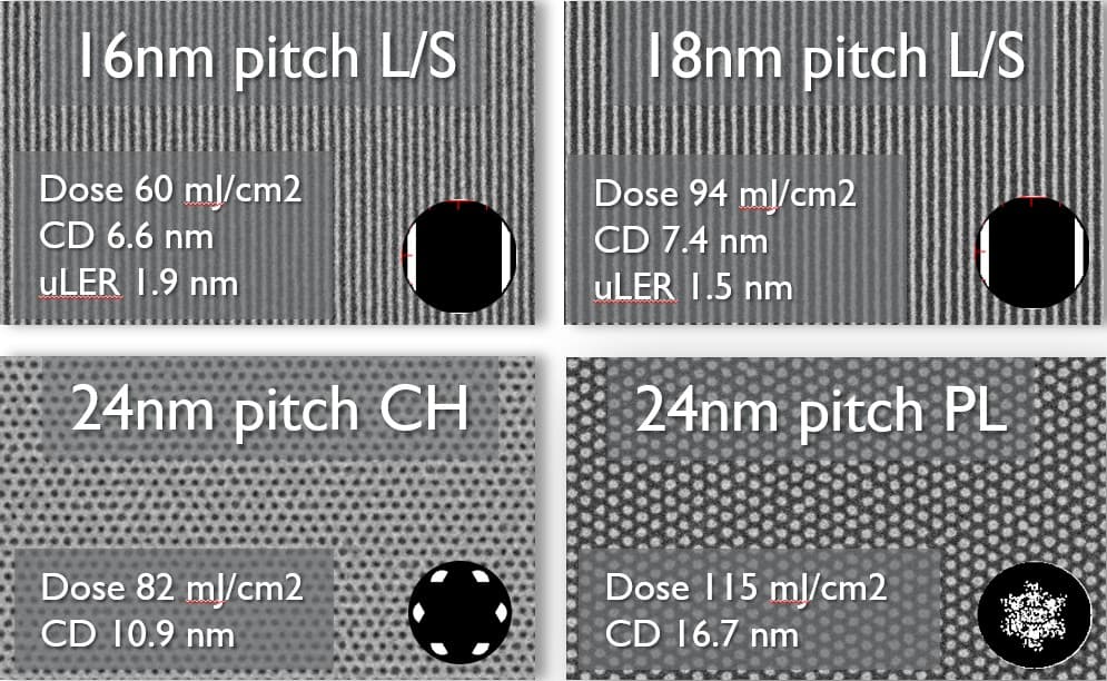
Figure 1 – (Top) 16nm and 18nm pitch lines/spaces (L/S), and (bottom) 24nm pitch contact holes (CH) and pillars (PL) after High NA EUV exposure.
The ultimate resolution is, however, a mere ‘optical’ promise, reflecting the quality of the aerial image before it hits the wafer. During wafer exposure, the aerial image creates patterns in the photoresist which, after resist development, are further etched into the underlying layers. The final resolution obtained on the patterned features therefore also depends on the performance of the materials (resists, underlayers, hard masks, etc.) and etch processes used during patterning. Process limitations may also impact the yield of the structures achieved across the 300mm wafer.
The High NA EUV resolution limit for yielding industry-relevant patterned structures will therefore be larger than 16nm pitch. Advanced litho material R&D work, with focus on novel materials and MOR enablement, is crucial to bringing the resolution of the patterning technology as close as possible to High NA EUV’s theoretical limit.
In 2025, imec demonstrated 20nm pitch yielding metallized line structures relevant for industrial damascene metallization, and 20nm and 18nm pitch Ru lines obtained with a direct metal etch (DME) metallization scheme [7].This aggressive resolution was achieved using a holistic approach, which involved co-optimizing optical proximity correction (OPC) techniques, photomask, resist, underlayer, and etch processes and materials.

Figure 2 – 18nm pitch Ru lines obtained with DME after single exposure High NA EUV lithography.
High image contrast improves local CD uniformity and reduces exposure dose
In a High NA EUV lithography scanner, the projection lens is hit by light having a greater number of diffraction orders than in a Low NA EUV scanner. This enhances the contrast of the aerial image – the difference in intensity between the light and dark areas after the light has passed the photomask – and is the reason behind the superior resolution. When the resist is exposed to an image with higher contrast, the printed features have better local CD uniformity (LCDU) and suffer less from roughness. This has been experimentally validated for various 29nm pitch hexagonal hole and pillar structures, showing LCDU gains between 18 and 42% with respect to 0.33NA printed features [5,6].
The high image contrast additionally lowers the dose to size required to print a pattern in the resist with sufficient quality. This in turn allows the exposure time to be reduced, which benefits scanner throughput and process cost. For the 29nm pitch holes and pillars, a ~60% dose-to-size gain could be demonstrated when using 0.55NA EUV lithography [5,6].
High NA EUV driver 2: process simplification
The chip industry may argue that features of 20nm can also be patterned with Low NA EUV lithography. True, but that can only be achieved by using complex multi-patterning steps. This involves splitting a chip pattern into two or more ‘simpler’ masks, which increases manufacturing time, reduces yield, enhances carbon footprint, and raises costs. The high resolution offered by High NA EUV lithography reduces the need for multi-patterning, allowing the smallest chip features to be printed in one single exposure.
Logic roadmap: single patterning of logic A14 and A10 critical metal layers
For A14 and A10 logic nodes, requirements for the most critical metal layers (i.e., M0 and M2) are very demanding: lines/spaces with ≤20nm pitches, aggressive tip-to-tip (T2T) structures to interrupt the lines (T2Ts with ≤15nm CD and ≤3nm LCDU as an industry target), and random vias with ≤30nm center-to-center distances. 0.33NA EUV lithography would require 3-4 masks to pattern these features, whereas 0.55NA EUV lithography can do this in one single exposure, as experimentally observed. Imec could also overcome the challenges in achieving good T2T control: a target LCDU below 3nm could be realized for 13nm T2T structures by co-optimizing source, mask (using low n phase shift masks), resist and etch (using directional etch techniques) [7].
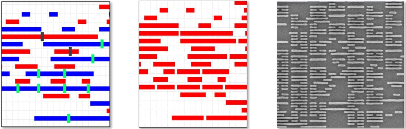
Figure 3 – (Left) While 0.33NA EUV lithography would require 4 masks to pattern metal A14/A10, (middle and right) High NA EUV lithography can print the same layout with only one mask.
DRAM roadmap: single patterning of D1d and D0a bitline peri / storage node landing pad layers
The ability to eliminate complex multi-patterning steps also makes High NA EUV lithography a roadmap enabler for future DRAM nodes, i.e., 32nm (D1d) and 28nm (D0a) DRAM. For these nodes, experiments have confirmed the feasibility of using High NA EUV lithography to pattern the BLP/SNLP layer – the layer that contains the bitline periphery and storage node landing pads [4]. While 0.33NA EUV lithography requires at least three masks for patterning these BLP/SNLP layers, 0.55NA EUV lithography can accomplish the same task with only one mask.
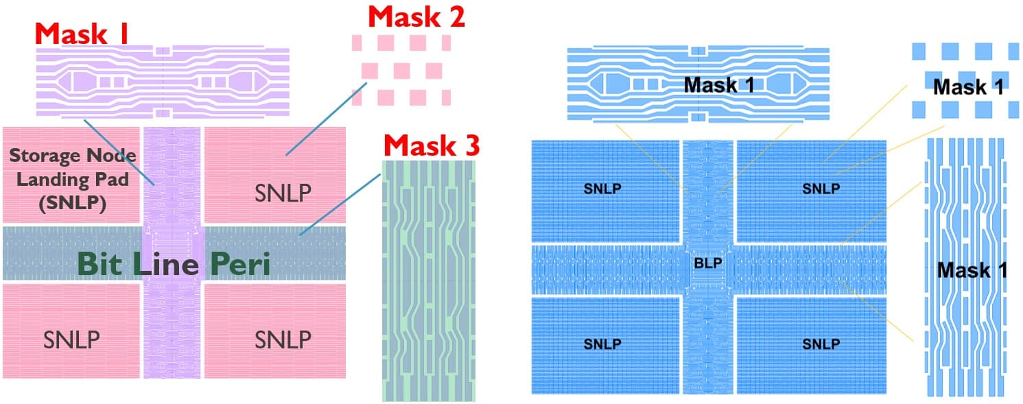
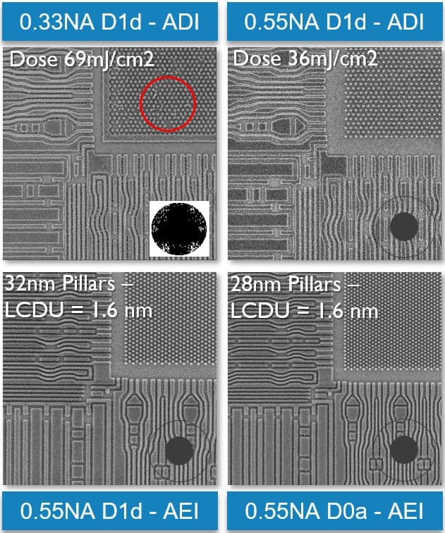
Figure 4 – High NA EUV lithography as a roadmap enabler for next-gen DRAM: (top left) while 0.33NA EUV lithography requires multi-patterning for D1d/D0a, (top right) 0.55NA EUV lithography enables single-patterning of the BLP/SNLP layer. (Bottom) TEM cross sections of 0.33NA and 0.55NA enabled BLP/SNLP layers (ADI = after development inspection; AEI = after etch inspection.)
High NA EUV driver 3: design flexibility
In the mid-to-late 2000s, designs for advanced logic chips moved away from 2D to 1D Manhattan-based circuit layouts in the most critical layers. This design ‘penalty’ was introduced to extend 193nm immersion lithography with lower k1 single patterning and multiple patterning, in anticipation of the readiness of 0.33NA EUV lithography.
In 2D bi-directional designs, Manhattan-based geometries are used to form the design along both vertical and horizontal directions. In contrast, 1D or unidirectional designs align structures to either vertical or horizontal directions per layer. Although 1D Manhattan offers a dense representation, it faces limitations. For example, when making an electrical connection from one metal line to a neighboring one, an extra layer with vias must be implemented – adding to the wafer cost, and to the path length of the electrical current.
The leap in resolution offered by High NA EUV lithography re-enables the use of 1.5D and 2D Manhattan designs, and makes it even possible to introduce curvilinear geometries and paths. This not only offers enhanced flexibility to chip designers to improve power and performance, but it can potentially reduce area consumption or cut down on the number of layers to reduce the cost.
High NA EUV enables bi-directional routing using 2D designs
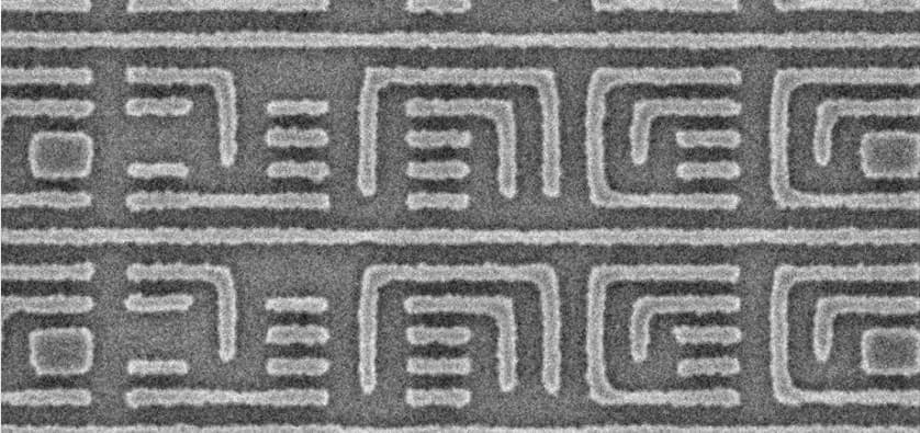
Imec and its partners demonstrated bi-directional routing using 2D Manhattan designs for 22nm and 28nm pitch line structures. OPC optimization and mask making quality enabled good after-etch pattern fidelity between design intent and wafer data for 2D designs [5,6].
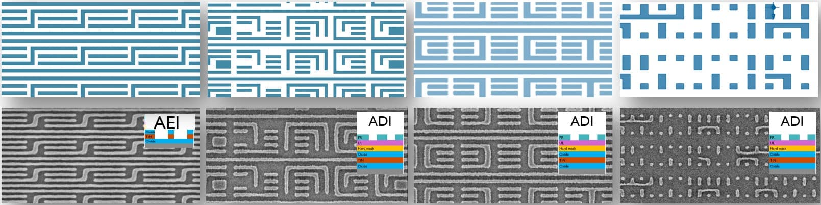
Figure 5 – High NA EUV lithography enables bi-directional routing via 2D designs, illustrated – from left to right – for a 22nm pitch 2 track skip; 28nm pitch N 2D; 28nm pitch C 2D and CFET middle-of-line routing exercise.
Compatibility with curvilinear design techniques
In addition, imec developed a solution for introducing more complex curvilinear geometries in the chip design phase, hence expanding curvilinearity beyond the OPC and mask phase [8]. Curvilinear design has been shown to be beneficial for multiple use cases, from standard cell design over source/drain contact and gate re-routing, to place-and-route designs. In standard cell designs, for example, it enables to relax M0 pitch while offering 20% area reduction. Imec recently demonstrated the compatibility of using curvilinear designed shapes with High NA EUV lithography, allowing for optimal use of the resolution leap offered by High NA EUV lithography at advanced nodes.
Conclusion
A holistic approach to developing High-NA-specific lithography and patterning technology is essential in validating its three major promises: resolution and image contrast gain over 0.33NA EUV lithography, process simplification through single patterning, and design flexibility through 1.5D, 2D, and curvilinear designs.
Imec and its ecosystem of partners continue to push these capabilities to the limit and develop the next generations of High NA EUV lithography and patterning technologies – offering balanced options to the industry. Ongoing R&D work includes tackling remaining challenges such as depth-of-focus improvement, stochastic defect mitigation, and stitching enablement.
As such, High NA EUV lithography technology will be a critical enabler for future technologies such as advanced AI chips, high-performance computing, and next-generation memory. It is seen as essential for keeping up with the demands of AI and data-centric applications, where hardware must evolve rapidly. The technology also plays a critical role in realizing the European Chips Act’s ambitions for enabling sub-2nm logic technology nodes.
This work has been enabled in part by the NanoIC pilot line. The acquisition and operation are jointly funded by the Chips Joint Undertaking, through the European Union’s Digital Europe (101183266) and Horizon Europe programs (101183277), as well as by the participating states Belgium (Flanders), France, Germany, Finland, Ireland and Romania. For more information, visit nanoic-project.eu.
This article was originally published in Semiconductor Digest.
Want to know more?
[1] ‘High-NA EUV lithography: the next major step forward,’ imec Reading Room, October 2021
[2] ‘Imec and ASML open joint High NA EUV Lithography Lab offering an early development platform to the leading-edge semiconductor ecosystem,’ imec press release, June 2024
[3] ‘Imec demonstrates readiness of the High-NA EUV patterning ecosystem,’ imec press release, February 2024
[4] ‘Imec demonstrates logic and DRAM structures using High NA EUV lithography,’ imec press release, August 2024
[5] ‘Patterning the Ångström future: High-NA EUV lithography breakthroughs,’ Geert Vandenberghe, imec ITF USA 2025
[6] ‘High-NA lithography at the turning point: preparing for industry insertion,’ G. Vandenberghe, Semicon Korea 2026 (February 11, 2026)
[7] ‘Imec achieves new milestones in single patterning High NA EUV lithography for both damascene and direct metal etch metallization processes,’ imec press release, September 2025
[8] ‘Curvilinear technology: a game changer for the logic technology roadmap,’ imec Reading Room, May 2025