What’s the environmental footprint of an integrated circuit? Today, this question is not easy to answer because the industry lacks a holistic approach to assess the impact of chip manufacturing accurately. By extending its design-technology co-optimization (DTCO) framework, imec has worked out a solution that estimates energy consumption, water usage, and greenhouse gas emissions of present and future logic CMOS technologies. A first analysis reveals an increase in each metric from node to node due to the growing complexity of chip technologies. The framework allows companies to make more sustainable manufacturing choices – far ahead of high-volume production. Imec presented these findings at the 2020 IEDM conference.
Environmental sustainability in the semiconductor industry: a growing priority
The semiconductor industry is resource-intensive in energy, water, chemicals, and raw materials. During manufacturing, various classes of emissions are being generated, including greenhouse gases such as CO2 and fluorinated compounds. To minimize the industry’s impact on the environment and to comply with local and global policies, environment, health and safety (EHS) control has become a critical component of every foundry for quite some time.
But due to growing concerns on climate change, resources depletion and global pollution, fabs and equipment suppliers want to make more efforts towards greener IC manufacturing. While EHS control is mainly limited to chemicals, abatement and water management, electronics companies want to know and reduce the full ecological footprint of their product. A reduced footprint might also guarantee business continuity – for example if scarce materials are involved – or give the company a competitive advantage. Today, companies rely on methods such as Life Cycle Assessment (LCA) to evaluate the environmental impact of their product from material sourcing to end-of-life.
The missing puzzle piece: life cycle assessment of (future) integrated circuits
Current LCA methods are however far from accurate and complete, especially when it comes to integrated circuits. The latest published information on mass balances and energy flows used in chip manufacturing relates to the 32nm technology node – a technology that was mainstream in the 2010 timeframe. Environmental data on the processing of present and upcoming CMOS technologies are hardly available. And what is known mostly stems from a partial view, coming from either the equipment or material supplier, or from what the foundry publishes after production. Fabless companies have no access to information at all. A holistic approach is lacking, making it extremely challenging to bring environmental considerations into the early technology definition stages.
A major stumbling block: the increasing complexity of future technologies
The task of estimating the environmental impact of CMOS technologies is greatly complicated by the increase in complexity from node to node. Through the years, novel materials, device architectures, processes and equipment have been introduced in all steps of chip manufacturing – including the front-end-of-line (FEOL), middle-of-line (MOL) and back-end-of-line (BEOL) – to ensure continuity of Moore’s Law. For future nodes, a myriad of options are being explored to further reduce logic cell area while increasing performance (i.e., operation frequency) from node to node.
To print ever tighter pitches, lithography techniques have evolved from single exposure 193nm (immersion) lithography to double, triple or quadruple patterning approaches. EUV lithography was made available for the 7nm node, allowing a strong reduction of the number of process steps. But not every foundry made that transition, as multiple processing routes are available for the same pitches. For future technology nodes, multiple EUV litho-etch sequences will be needed for printing pitches below 30nm.
In the FEOL, the FinFET has become the mainstream device architecture for the 7nm technology node – the most advanced node that is currently being used for chip production. For the next technology nodes, imec sees (vertically stacked) lateral nanosheets as the way forward, followed by the forksheet device architecture and the complementary FET (CFET).
To keep up with area scaling in the front-end, BEOL dimensions have been reduced at an accelerated pace – leading to ever smaller metal pitches and reduced cross-sectional areas of the wires. Through the years, the number of interconnect layers and the complexity of the densest metal lines has significantly increased. New process schemes for metallization are being explored, and new metals are being introduced to reduce the resistivity in the densest layers.
From ‘happy scaling’ to design-technology co-optimization
Along with this evolution came DTCO: design-technology co-optimization. Until around 2005, the semiconductor community lived in an era of ‘happy scaling’. The continual shrinking of transistors yielded benefits for the whole system in terms of power consumption, performance, area and fabrication cost (denoted as PPAC). But since 2005, the awareness grew that benefits could only be maintained if device technology and design would be co-optimized together. DTCO, supported by the introduction of scaling boosters, allows a further shrink of the area, not at transistor but at standard cell level. Scaling boosters, such as self-aligned gate contact or buried power rail, further improve connectivity between the different parts of the chip, but also impact chip production at the level of FEOL, BEOL and MOL.
DTCO including sustainability: the imec approach
The DTCO framework as explained above can be an interesting base for analyzing environmental indicators that can be monitored in parallel to the standard PPAC metrics. DTCO takes process flows for present and future IC technologies into account. These can be coupled to relevant environmental information on process steps and equipment, allowing for a power-performance-area-cost-environmental (PPACE) score analysis.
Imec has used electrical energy consumption, ultrapure water usage and greenhouse gas emissions as the main metrics for evaluating environmental impact. To extend the DTCO framework with these metrics, the imec team used data from its own 300mm fab, complemented with information coming from its ecosystem of equipment suppliers. This way, different knowhow could be connected.
The aim is to perform a PPACE analysis of different scaling choices already in the pathfinding phase to identify bottlenecks, risks and opportunities ahead of high-volume manufacturing. A true holistic approach is required to conduct correct evaluations. For example, EUV tools are known to consume approximately ten times more power per tool than traditional 193nm (immersion) lithography tools. But EUV will also significantly reduce the number of processing steps, which must be taken into account when deriving the total envelop of power usage.
Imec used the extended DTCO framework to quantify and benchmark different process flows and integration schemes, from the 28nm until the 2nm node. Next, it was demonstrated how the framework can be used to make more sustainable manufacturing choices.
General trend: increase in energy, ultrapure water and greenhouse gas emissions
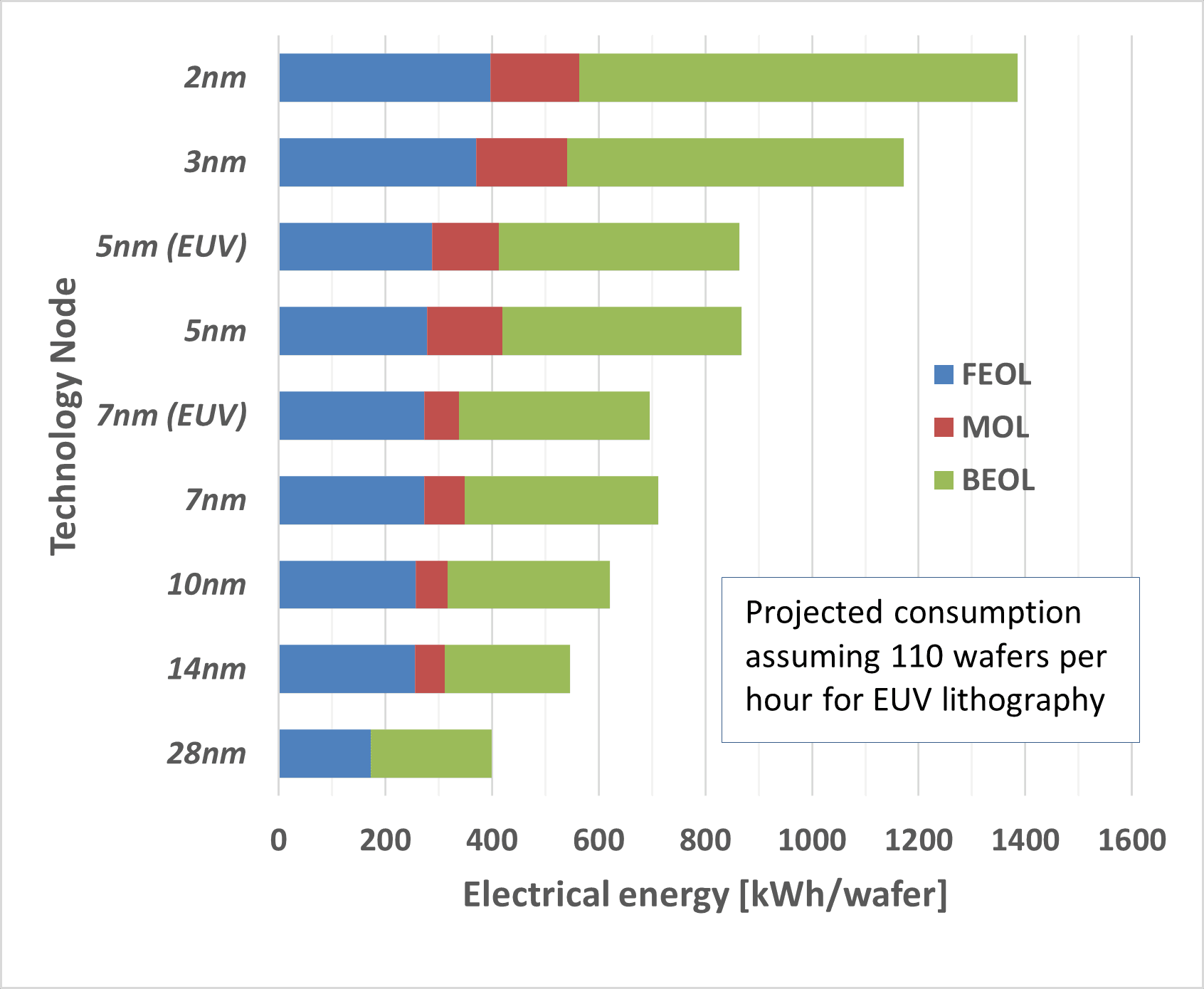
Technology scaling continues to bring benefits in transistor density and higher speed. In parallel, for the assumptions made in this work, the PPACE analysis shows a significant increase in electricity (x3.46) and ultrapure water consumption (x2.3), and in greenhouse gas emissions (x2.5) per wafer from the 28nm to the 2nm node. A more detailed evaluation reveals that this increase per wafer is indeed due to the growing complexity from node to node, i.e. the growing the number of process steps, the introduction of scaling boosters, an increase in the number of metal lines, and the necessity of applying multiple patterning techniques. At transistor level, the environmental metrics are observed to reduce due to further standard cell area scaling and performance improvement. But the reduction saturates for the 3nm and 2nm technology nodes.
Looking at the results per metric, the analysis can be refined to trace the biggest contributors. The energy consumption per wafer – derived from summing the electrical energy usage of individual process steps – increases in the three parts of the process, i.e. FEOL, BEOL and MOL. When looking at the FEOL, for example, the gate module manufacturing seems to be the biggest contributor.

Electrical energy usage for the different technology nodes, showing an increase in energy consumption for the FEOL, MOL and BEOL. The energy consumption was derived from the equipment’s real average power multiplied by tool times.
Ultrapure water is used in semiconductor manufacturing for rinsing the wafers in wet benches and in chemical mechanical polishing (CMP) steps. As these steps largely increase in number from node to node, ultrapure water consumption more than doubles.
A similar increase is observed for greenhouse gas emissions. Greenhouse gases such as fluorinated compounds are mainly used for dry etching, for the cleaning of chambers used for chemical vapor deposition (CVD) and during epitaxial growth. Main contributors are SF6 and NF3, gases with a high global warming potential. A growing number of CVD steps from node to node translates into a larger NF3 usage. This increases the overall CO2 equivalent – a metric that allows to compare emissions from various greenhouse gases based on their global warming potential.
Estimated equivalent CO2 emissions from greenhouse gases used in process flows across different nodes.
There is of course an uncertainty in the technology choices that a fab will make from the 5nm node onwards. In our calculations, we assumed for example the introduction of EUV lithography in the BEOL, the insertion of scaling boosters such as buried power rail, and the transition to the nanosheet device for the 2nm node. The framework can be used to evaluate other technology scaling scenarios as well, but these should be evaluated in combination with the projected functionality and performance of the chosen technology.
Two specific cases: NF3 abatement and EUV throughput
Some of the assumptions made in this work may greatly vary from fab to fab. For example, the electricity usage as derived from this analysis can be used to derive equivalent CO2 emissions. Of course, these emissions depend on the sources used for electricity generation. In this work, these sources were assumed to be fixed. But as foundries transition from fossil fuel-based electricity generation to renewable energies, the node-to-node growth of the electricity carbon footprint per wafer needs to be compensated for. The team therefore conducted several sensitivity analyses, determining how the target metrics are affected based on changes in the input variables.
An example is the evaluation of the abatement factor for the NF3 greenhouse gas, which was assumed to be 95%. This means that 95% of the NF3 gas that is used within the fab is burnt or converted to prevent it from getting in the environment. But by changing the abatement factor to 99% (as announced for the latest abatement systems), the total greenhouse gases would stay close to the target set by the International Technology Roadmap for Semiconductors (ITRS) in 2015.
The extended DTCO framework can also be used to set targets, helping companies to make greener manufacturing choices. Take for example EUV lithography. On the one hand, EUV tools consume more power per tool than 193nm lithography. The throughput of EUV – expressed in wafers per hour – is also lower than for 193nm lithography, enlarging the energy consumption envelop. But on the other hand, EUV single patterning significantly reduces the number of process steps when compared to using 193nm lithography in combination with complex multi-patterning techniques such as self-aligned quadrupole patterning (SAQP). The new framework reveals that a target throughput of 110 wafers per hour for EUV is needed to reach the same electrical energy usage as for SAQP when patterning critical BEOL metal lines.
Impact of EUV on (left) process complexity and (right) electrical energy usage. With a throughput of 110 wafers per hour, the total energy usage of EUV is close to the energy of 193nm ArFi lithograpy in combination with SAQP. (SADP=self-aligned double patterning; SAQP=self-aligned quadrupole patterning; LE=litho etch.)
Future plans
To get the full ‘environmental picture’, the impact of raw materials extraction and refinement should be included into the DTCO framework as well. The first initiatives in this direction have been taken. In this context, the team will also look at the impact of adopting new materials in the process flows, especially when they are listed as critical. For these materials, options of using recycled materials or improving process tools for minimal material usage can be taken into consideration.
The team also plans to use the extended DTCO framework for evaluating the PPACE metrics for other technologies, including non-volatile and volatile memories. In addition, the framework will gradually be extended towards the system level – by including metrics related to packaging, 3D ICs, printed circuit boards and overall systems.
This article was originally published in EETimes.
Want to know more?
More details can be found in the invited 2020 IEDM paper ‘DTCO including sustainability: power-performance-area-cost-environmental score (PPACE) analysis for logic technologies’, presented by M. Garcia Bardon et al. (available after the IEDM conference). Interested in receiving the paper? Fill in our contact form.

Marie Garcia Bardon received the Ph.D. degree in microelectronics from the Katholieke Universiteit Leuven in collaboration with imec in 2010. She is now senior researcher at imec, modelling and benchmarking emerging devices and technologies for logic and memory applications. She has specialized in holistic pre-silicon evaluation and design-technology co-optimization including electrical and process aspects, working together with circuit, device and process integration colleagues and imec industrial partners.

Bertrand Parvais is a principal member of the technical staff at imec, in charge of RF and mmWave device technologies. He received his electrical engineering and Ph.D. degrees from the Université Catholique de Louvain, Louvain-la-Neuve, Belgium, in 2000 and 2004, respectively. He joined imec as a device engineer, working on the characterization and modeling of transistors in advanced CMOS technologies for analog and RF applications. From 2009 to 2016, he was involved in designing mixed-mode and millimeter-wave CMOS circuits. Since 2016, he has led imec research teams working on transistor compact models and RF transistor technologies. In parallel, he joined the Vrije Universiteit Brussels (VUB) in 2017 as a guest professor.
More about these topics:
Published on:
17 December 2020


