Computing power needs are exploding due to the rapid rise of digital applications and data processing. With the growing use of artificial intelligence to tackle the major challenges of our time, like climate change or food shortage, the computing need is expected to double every six months from now on. To handle the exponentially growing amounts of data in a sustainable way, we need improved high-performance semiconductor technology. In order to achieve that, we need to address five challenges simultaneously. While no company in the world can accomplish this alone, co-innovation and collaboration across the semiconductor ecosystem will enable the continuation of Moore’s law: that is the key message from imec's ambitious roadmap for the upcoming 15 to 20 years.
Five walls at a time
The scaling wall: pure lithography-enabled scaling is slowing down. It is becoming increasingly difficult since individual structures of microchips and transistors are approaching the size of atoms, where quantum effects begin interfering with the operation of microchips.
The memory wall: system performance is confronted with data path limitations between the cores and the memory. In fact: memory bandwidth cannot keep up with processor performance. We have more flops per second than gigabytes per second.
The power wall: it is becoming more challenging to bring power into the chip and extract heat from the chip package, so we will have to develop improved power delivery and cooling concepts.
The sustainability wall: the manufacturing of semiconductor devices contributes to an increasing environmental footprint, including greenhouse gas and water, natural resources, and electricity consumption.
The cost wall: obviously, chip manufacturing costs may explode with the complexity increase, together with the costs for design and process development.
Tearing down the walls
At first sight, things don’t look great for the prophecy of Gordon Moore, who first noted that the number of transistors in a dense integrated circuit (IC) doubles about every two years. This prognosis is especially true if we stubbornly stick to Dennard scaling and traditional Von Neumann compute architectures. In its scaling roadmap, imec proposes an alternative path for the future of chip technology, with fundamental changes in architectures, materials, new basic structures for transistors, and ... a paradigm shift. The imec roadmap will take us from 7 nm to 0.2 nm or 2 ångström by 2036, keeping an introductory pace of two to two-and-a-half years.
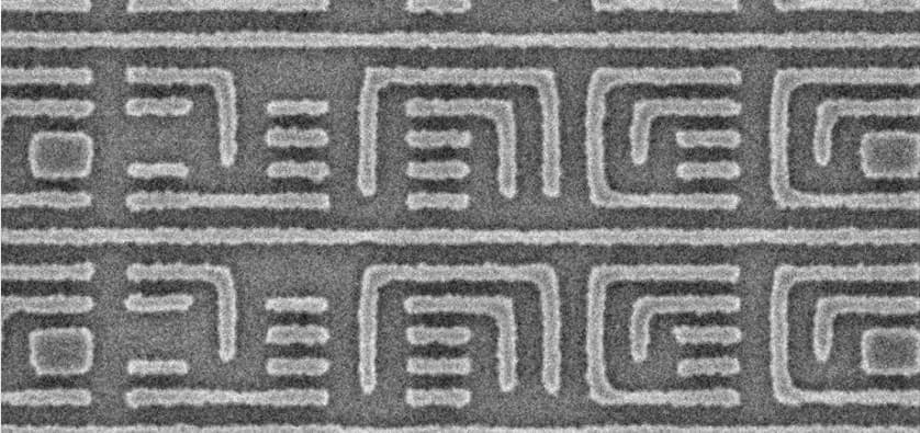
First, the continuous advances in lithography will be key to further dimensional scaling: traditional lithography uses light, and, today, the wavelength of light is greater than the required accuracy of the patterns. That’s why Extreme UV (EUV) lithography has been introduced. It is now appearing on more and more functional production belts for volume manufacturing. EUV will take us from the five nanometer-generation to two nanometers. To go smaller we need an updated version of EUV, high-NA EUV, with bigger lenses. These will have a diameter of one meter with an accuracy of 20 picometers. For high-NA EUV, the first prototype, which is being developed by ASML, will be available in 2023. Insertion in high-volume manufacturing is expected sometime during 2025 or 2026. In order to derisk the introduction in manufacturing, imec, together with ASML, has set up a very intensive program to develop all the key enabling building blocks, such as the mask technology and materials using wet or dry UV resist, metrology, and optics characterization.
At the same time we will also need innovation in the transistor architecture. Today almost all chip manufacturers build microchips with FinFET transistors. However, when entering the 3nm-generation, FinFETs suffer from quantum interference, causing disruptions in the operation of microchips.
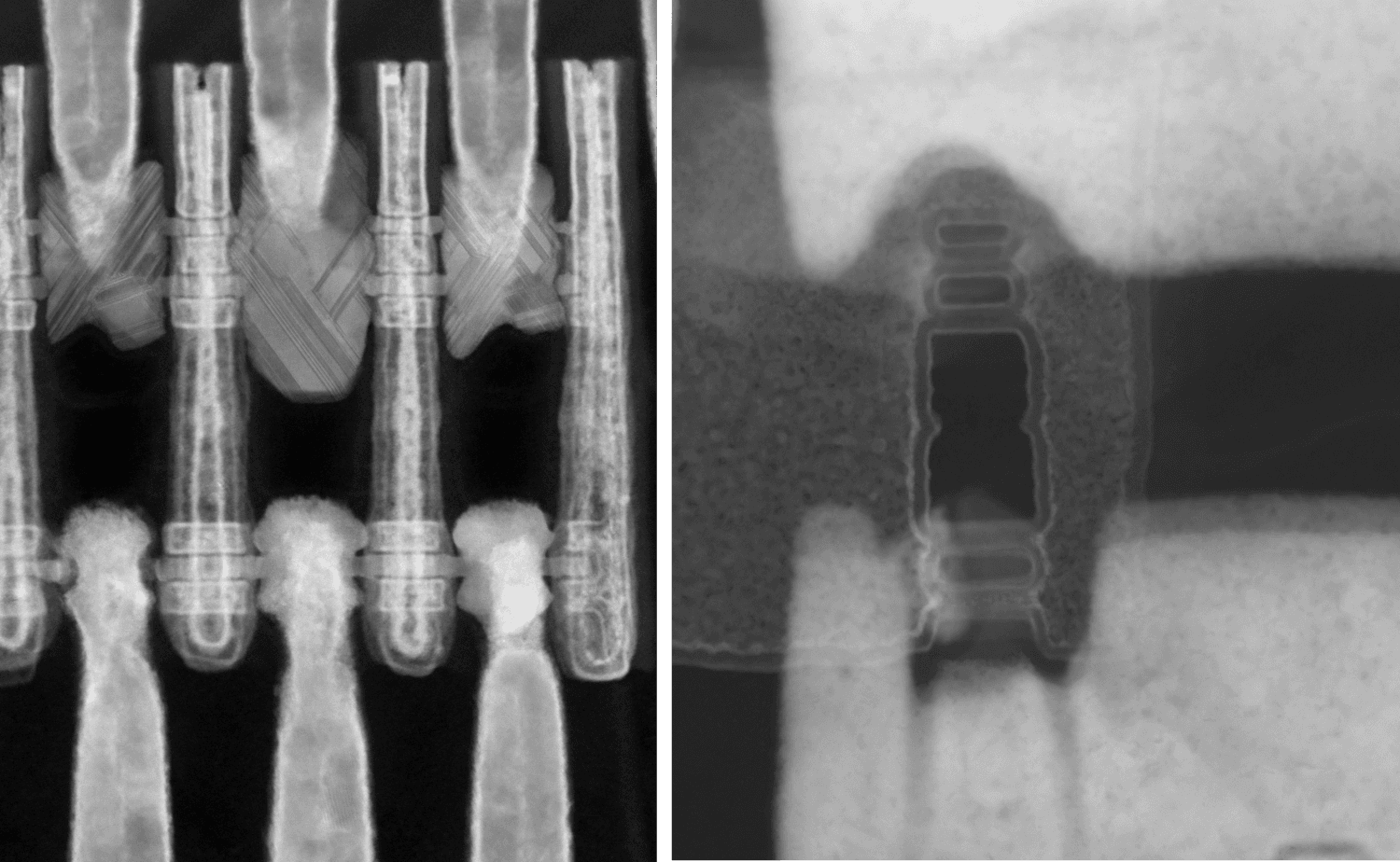
Next in line is the Gate-All-Around (GAA) or nanosheet transistor, built up as a stack of nanosheets, it will offer improved performance and improved short channel effects. This architecture will be essential from 2 nm onwards. Major chip manufacturers like Samsung, Intel, and TSMC have already announced that they will introduce GAA transistors in their 3nm and/or 2nm nodes. The forksheet transistor is an imec invention, even denser than the nanosheet transistor, extending the gate-all-around concept to the 1 nm generation. The forksheet architecture introduces a barrier between the negative and positive channels, enabling the channels to come closer together. This architecture is expected to enable a cell-size shrink of 20 percent.
Further scaling can be realized by putting the negative and positive channels on top of each other, referred to as the Complementary FET (CFET) transistor, a complex vertical successor to the GAA. It significantly improves density but comes at the expense of increased process complexity, especially to contact the source and drains of the transistors.
In time, CFET transistors will incorporate new ultra-thin 2D monolayer materials with an atomic thickness, like Tungsten disulfide (WS2) or molybdenum. This device roadmap, combined with the lithography roadmap, will bring us to the ångström age.

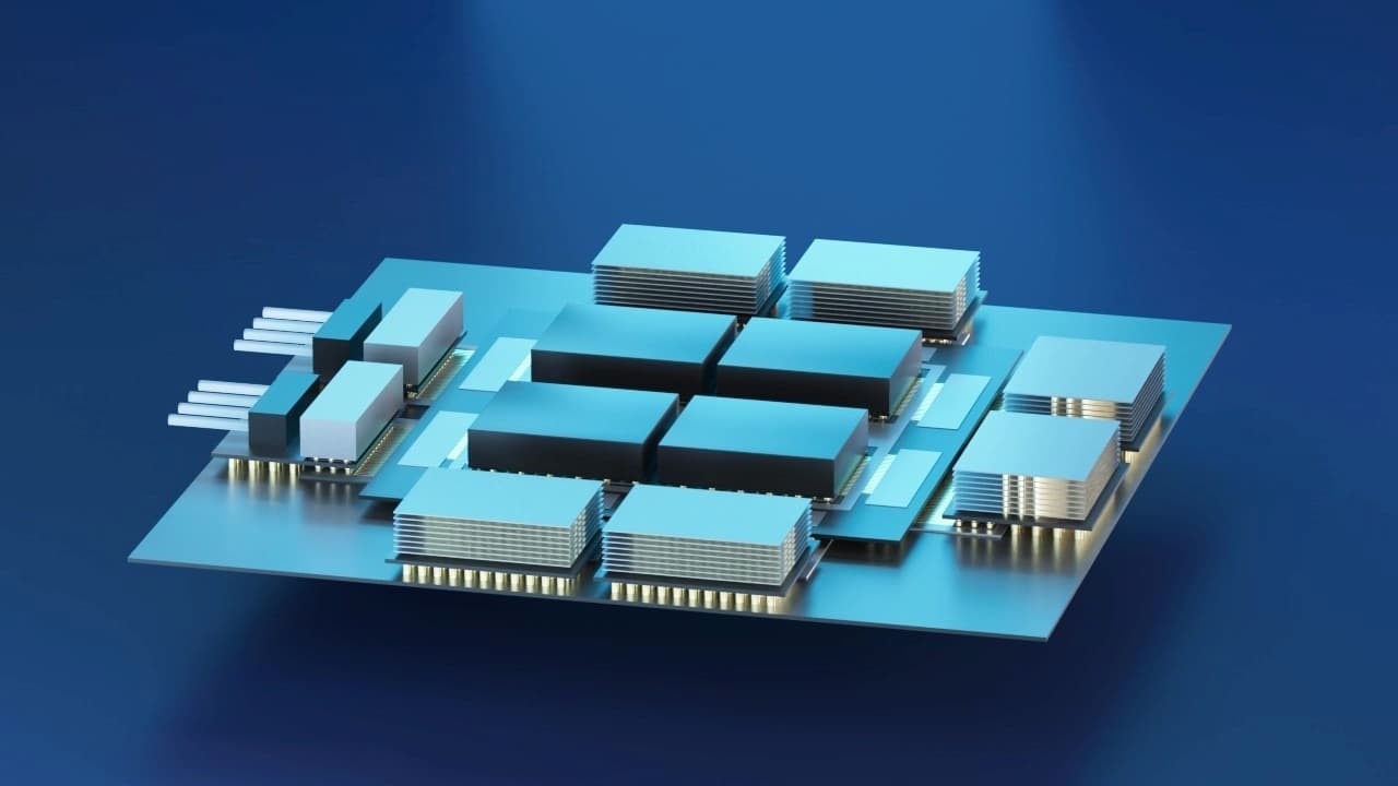
Two other challenges are playing at the system level of these sub 2nm-transistors. The memory bandwidth cannot keep up with CPU performance. The processor can't run faster than the pace at which data and instructions become available from the memory. To knock down this ‘memory wall’, memory must come closer to the chip. An interesting approach for tearing down the memory wall is 3D system-on-chip (3D SOC) integration, which goes beyond today's popular chiplet approaches. Following this heterogeneous integration approach, the system is partitioned into separate chips that are concurrently designed and interconnected in the third dimension. It will allow for example to stack a SRAM memory layer for level-1-Cash right on the core logic devices, enabling fast memory to logic interaction. To achieve extreme high bandwidth off-module connectivity, optical interconnects, integrated on photonics interposers are being developed.
Regarding system-related challenges, getting enough power into the chip and getting the heat out becomes more difficult. However, a solution is in sight: the power distribution now runs from the top of the wafer through more than ten metal layers to the transistor. Imec is currently working on a solution from the backside of the wafer. We will sink power rails into the wafer and connect them to the backside using nano-through-silicon vias in wider, less resistive materials. This approach will decouple the power delivery network from the signal network, improving the overall power delivery performance, reducing routing congestion, and, ultimately, allowing further standard cell height scaling.
Finally, semiconductor manufacturing comes at a price. It requires large amounts of energy and water and creates hazardous waste. But the entire supply chain needs to commit to tackling this problem, and an ecosystem approach will be essential. Last year, imec launched its Sustainable Semiconductor Technologies and Systems (SSTS) research program, which brings together stakeholders of the semiconductor value chain—from large system companies, like Amazon, Apple and Microsoft, to suppliers including ASM, ASML, KURITA, SCREEN, and Tokyo Electron. The goal is to reduce the carbon footprint of the entire industry. The program assesses the environmental impact of new technologies, identifies high-impact problems, and defines greener semiconductor manufacturing solutions early on during technological development. It allows us to make informed choices when we move to future technology generations and develop new processes.
Paradigm shift
In the long term, the Von Neumann architecture needs an overhaul. Professor Von Neumann saw the digital computer as a system with input, a central processing unit, and an output. But we will need to evolve toward domain-specific and application-dependent architectures, with massive parallelization comparable to the way our human brain works. This implies that the CPU will have a smaller role in favor of custom-made circuits for specific workloads.
This paradigm shift, in addition to the walls ahead, marks the beginning of interesting times in the semiconductor industry. We will need co-innovation and collaboration across the entire semiconductor ecosystem: foundries, IDMs, fabless, fab-lite, equipment & material suppliers. Not just to meet Moore’s law for the sake of it, but because semiconductors are at the core of the performant deep technology applications that can make impactful progress in tackling the challenges of our time like climate change, sustainable mobility, air pollution, and food shortage. The stakes are high.
More about these topics:
Published on:
2 February 2023


