Why are we looking to an STCO approach when developing future technologies?
Julien Ryckaert: “The entire semiconductor industry is currently going through a great transformation. For more than a decade now it is clear that the dimensional scaling inspired by Moore’s and, more specifically, Dennard’s Law cannot be used as a barometer to predict the future of CMOS technology nodes.
This stems from several factors to which we now refer as ‘scaling walls’. Not only is it becoming extremely difficult and expensive to scale the feature dimensions of CMOS components, but industry is also facing severe power and speed roadblocks in their complex systems.
At the technology level, new device architectures and scaling boosters – supported by design-technology co-optimization (DTCO) – could maintain some area scaling in the next couple of CMOS nodes. But these will inevitably run out of steam, or at least will not suffice in providing the system scaling expectations of future applications.
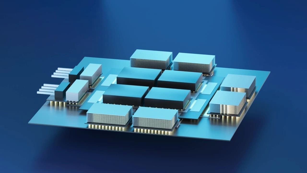
At the architecture level, complex memory hierarchies, multi-core, and multi-threading as well as core specialization (xPUs...) on a single system-on-chip (SoC) or in chiplets have become the way to overcome these scaling walls.
The problem we are facing today is that few of the earlier innovations have been the result of a true system-architecture-to-technology optimization loop.
The problem we are facing today is that few of these innovations have been the result of a true system-architecture-to-technology optimization loop. The biggest challenge moving forward will be in addressing the right technology ingredients that can unlock the major system scaling bottlenecks. But also in exploring how some technology disruptions can enable new ways of computing. This is the purpose of a system-technology co-optimization (STCO) framework.”
How will imec contribute to STCO?
“Imec is naturally situated on the technology side of the ecosystem, that’s where it has shone for decades and provides a true differentiation in the ecosystem. However, as we need to take a leadership position in defining the technology of the future, we must now enrich our technology roadmap with system scaling challenges.
This evolution fundamentally means we need to step out of our traditional ‘general purpose’ technology offering and embrace the fact that solutions are driven by application-specific requirements such as AI, high-performance computing (HPC), AR/VR, ...
We need to step out of our traditional ‘general purpose’ technology offering and embrace the fact that solutions are driven by application specific requirements.
Moreover, an optimal system implementation will be the result of a subtle optimization across multiple technologies such as extreme CMOS logic scaling, advanced 3D packaging, novel memory elements and even Si photonics. These different technology research activities have up to now been conducted separately, each with their own DTCO research and roadmap.
To prepare ourselves for the system-driven scaling transition, we have reorganized our core program offering and integrated all DTCO activities into one single program that will study technology-to-circuit optimization across all core technology programs. We have complemented this DTCO program with a STCO program that will ensure the liaison between the DTCO research and the system application space.
The goal of this STCO program is to translate future system needs and bottlenecks into technology requirements in a top-down approach. It will also explore the possibility to enable new architectures leveraging unique and novel technology capabilities.”

Schematic representation of the STCO framework.
What progress are we making in STCO today? Can you back that up with some recent examples?
“In each of our core technology programs we have started isolated research activities that already required some level of system evaluation.
A good example is the backside power delivery network that we presented at the 2022 VLSI Symposium. This work was the result of 3D program activities and logic activities working together to develop a system solution to power delivery. The backside technology heavily affects the logic scaling roadmap as much as it requires 3D technology capabilities such as wafer handling and through-silicon via (TSV) processing. But understanding why and how a backside power delivery network can bring true system performance benefits requires assessing its behavior in a more complex environment and diving deeper into system configurations. In 2021, in IEEE Spectrum, imec and Arm reported the system-level benefits of a backside power delivery network with buried power rails at processor design level.
Another example is emerging memories, some of which are envisioned to replace on-chip SRAM. Such a memory solution will inevitably affect the logic scaling roadmap and can only be evaluated in a system simulation framework. Not to mention that some of these memories may be stacked in 3D.
Technology research in the logic, memory and 3D programs can no longer be treated in separate ‘silos’.
As soon as we started tackling system-level challenges for these examples, we quickly realized that, for each example, all technology solutions are entangled with each other. It became clear that technology research in the logic, memory and 3D programs could no longer be treated in separate ‘silos’: it must be done concurrently and driven by system application targets.
The good thing is that we are not starting from scratch as we already have many research activities that are analyzed from a system perspective. What we need now is to structure these activities into a common vision and derive a roadmap for them.”
What can we expect in the next few months?
“Our DTCO/STCO activities are articulated around 3 essential scaling walls for systems: the memory/bandwidth wall (i.e., how to get data at enough speed to feed the logic cores), the power/thermal wall (i.e., how to efficiently handle power delivery and thermal dissipation) and the dimensional scaling wall.
We do see a lot of excitement around this initiative even if people measure as much as we do that it is an ambitious program goal.
We will need of course to calibrate this research roadmap with our partners and make sure we are working on the right challenges for the industry. This will require in depth discussions with all our partners, and these have already started taking place. We do see a lot of excitement around this initiative even if people measure as much as we do that it is an ambitious program goal. We will have to be smart in choosing our battles, those that are the most relevant for the scaling of future systems while leveraging our unique technology capabilities.”
What makes imec unique for the global semiconductor industry in setting up this STCO program?
“A true STCO research requires the integration of many disciplines together, each dealing with widely different scales and operating their science at different domains of abstraction. A true challenge is then to build a proper set of abstraction layers from one domain to another without losing critical information along the way. This is the only way to propagate information from top to down and bottom to up in order to perform a complete system optimization.
Imec holds a unique infrastructure where most of the required disciplines sit under the same roof working closely together.
To do this properly, you not only need all the right expertise in each domain, but you also need these disciplines to closely interact with one another. Imec holds a unique infrastructure where most of these disciplines sit under the same roof working closely together. This facilitates the exchange of ideas, the smooth propagation of information and the broadening of a critical eye on the results and interpretations.
I feel strong excitement moving forward in this STCO space as we all, no matter which area we come from, understand that making the difference in the future of semiconductor research will be through an STCO framework. And imec is the right place for such an initiative to take off.”

Julien Ryckaert received an M.Sc. degree in electrical engineering from the University of Brussels (ULB), Belgium, in 2000 and a Ph.D. degree from the Vrije Universiteit Brussel (VUB) in 2007. He joined imec as a mixed-signal designer in 2000, specializing in RF transceivers, ultra-low power circuit techniques, and analog-to-digital converters. In 2010, he joined the process technology division in charge of design enablement for 3DIC technology. Since 2013, he oversees imec’s design-technology co-optimization (DTCO) platform for advanced CMOS technology nodes. In 2018, he became program director focusing on scaling beyond the 3nm technology node and the 3D scaling extensions of CMOS. Today, he is vice president of logic and in charge of compute scaling.
More about these topics:
Published on:
12 December 2022


