Ab initio modeling of EUV photo resists
Leuven | More than two weeks ago
Using state-of-the-art quantum mechanical modeling to develop the chemistries for next angstrom scale patterning.
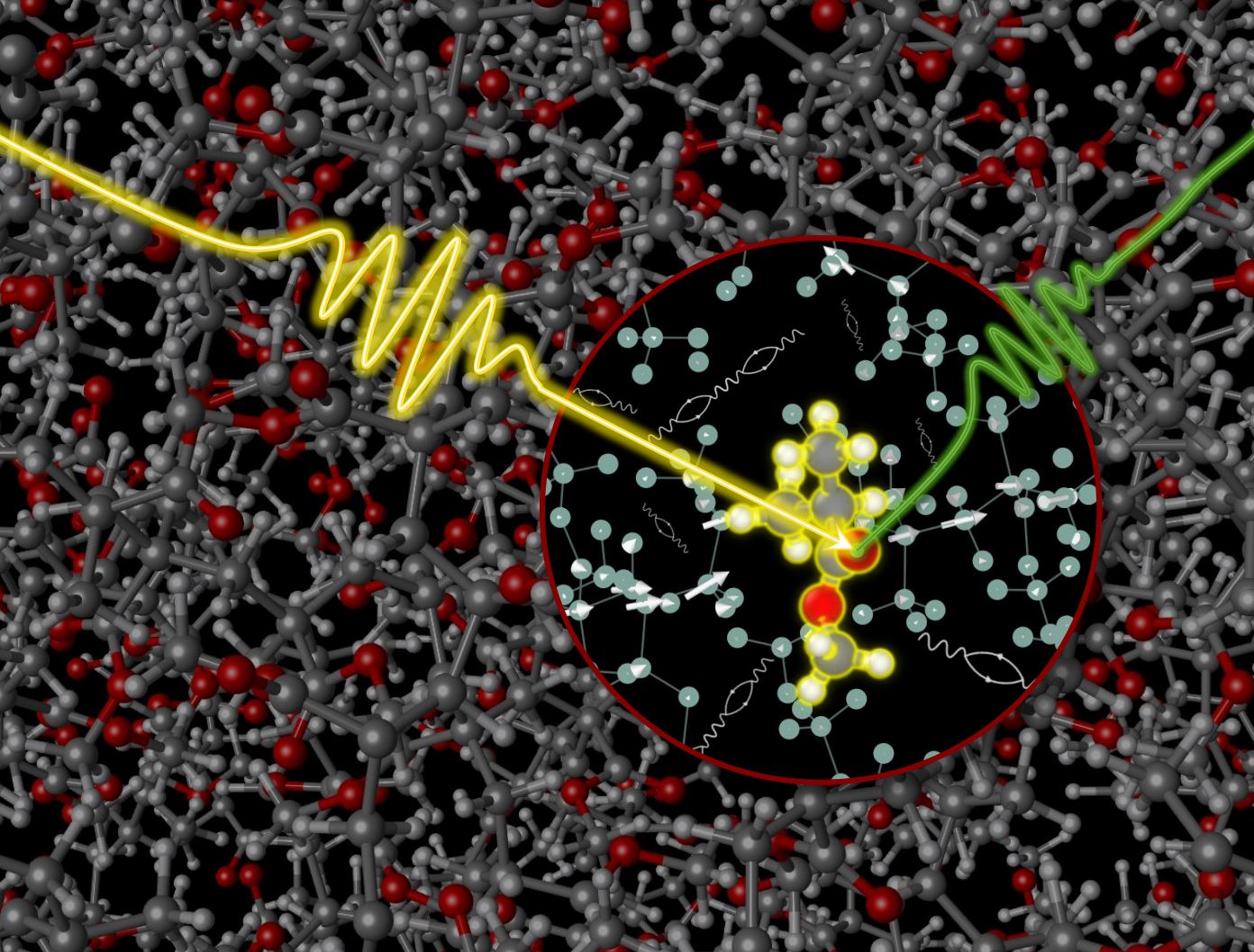
For many decades, progress in the electronics industry has been, and is still, driven by the miniaturization of integrated circuits (ICs). Besides getting smaller the circuit designs are also getting more and more complex. Creating the patterns to realize these circuits on a chip is performed by using photolithography. In photolithography a chemical photoresist is irradiated by laser light in the desired pattern. After washing away the non-reacted residue, the layer below the areas that are not protected by the reacted photoresist can be etched to form the desired pattern. The wavelength of the laser light ultimately restricts how small the dimensions of the printed patterns can be made. To produce the patterns of the next generation electronics we will need to use 13nm laser light. This light has an energy of 92eV and does not directly interact with the valence electrons, which participate in chemical bonding, but first with much more strongly bound core electrons. Working at these high energies, therefor, makes for a much more complex chemistry. Developing a better understanding of this chemistry is essential to enable the next generation of electronic devices.
To investigate photoresist chemistry at EUV energies, imec has built a new lab, the AttoLab. At the AttoLab, the spectroscopic properties of the photoresists can be followed starting from only tens of attoseconds after the interaction with an EUV pulse. Changes in the various spectra indicate the occurrence of a reaction step or any other change in the material. However, determining what happened at the atomic level from the spectra alone is far from trivial. By comparing the measured spectra to results from quantum chemical calculations we can assign certain states of the material to specific spectra and so understand which reactions take place. Performing these calculations, making the comparisons, and modeling the full process will eventually develop the much-needed understanding of what happens in EUV photoresists and is the topic of this PhD. project.
In the cause of this project the PhD. student will be performing state of the art ab initio calculations. Performing this correctly and efficiently requires a proper understanding of the theoretical concepts on which the methods are based and on the way they are implemented in computer code to be executed on super computers. Which calculations to perform also requires an understanding of the relevant chemistry. During the project the understanding and the necessary skills will be trained at imec.
To be eligible, applicants must have a master degree in either physics or chemistry focusing on the theoretical aspect. Due to the complexity and the high amount of individual calculations, an efficient and robust automation and data processing infrastructure is essential. We continuously develop and improve such an infrastructure for all our calculations, written in python. Good knowledge of this language is hence required. A strong motivation, a good knowledge of solid-state physics or quantum chemistry and UNIX/LINUX are a plus. Excellent writing and oral communication skills are desired.

Required background: Master in Physics, Chemistry, or equivalent
Type of work: Theoretical in direct collaboration with experimentalists
Supervisor: Daniel Escudero
Co-supervisor: Geoffrey Pourtois
Daily advisor: Michiel van Setten
The reference code for this position is 2025-023. Mention this reference code on your application form.
