Advanced thermal management of wafer-level optical interconnects in next-gen AI/ML systems
Leuven | More than two weeks ago
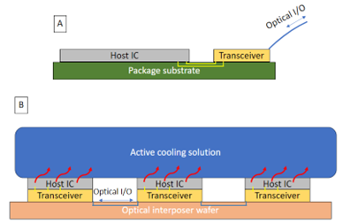
Over the past decade, Silicon Photonics (SiPho) has emerged as a key enabling technology for datacenter optical interconnectivity and is now considered to enable high-bandwidth optical interconnectivity networks in future high-performance computing (HPC) and machine learning (AI/ML) systems [1]. In the pursuit of minimizing interconnect parasitic losses, the optical transceiver is being integrated as close as possible to the host IC. With this in mind, the co-packaged optical module (CPO) was introduced (Fig.1, A), where the optical transceiver is integrated directly adjacent to the host IC on the same interposer substrate. Taking this one step further, 3D integration by die stacking of an active SiPho transceiver die on a host IC can be done. This highly integrated approach opens the opportunity for optically interconnecting multiple GPU/CPUs on an optical interposer wafer (Fig.1, B) [2]. Current optical I/O links based on SiPho technology are however significantly affected by changes in local and ambient temperature variations, e.g. caused by the highly non-uniform power generation in the host IC, the laser sources, and the optical devices themselves. This introduces thermal management challenges: high levels of thermal cross-talk between the host IC and transceiver are expected, which could detune optical resonance-based devices. Combining multiple high-power CPU/GPUs (>700 Watt) on an optical interposer wafer leads to a high thermal load of tens of kW which has to be removed with adequate active (liquid) cooling solutions.
The objectives of this PhD are to investigate the thermal behaviour of the Si photonics devices in this wafer-level system in terms of heater efficiency and thermal cross-talk to all other components), and to develop an effective thermal management solution for this photonic network-on-wafer systems that enables: 1) limiting the operating temperature below the allowed maximum value for all the logic, memory and optical components in the system and 2) control the waveguide temperature in the SiPho devices.
In this PhD work, the following activities are foreseen:
- The development of multiscale thermal models to simulate wafer-level thermal effects (tens of cm) down to device-level thermal cross-talk and heater efficiency (µm scale).
- Investigate advanced (liquid) cooling solutions for high thermal loads (>10 kW) and their integration in wafer-level assemblies.
- Experimental validation of the thermal models and experimental thermal and optical characterization using test structures.
- Obtaining the experimental data as well as required inputs for the simulations will be done in close collaboration with experts from multiple imec research programs, such as optical I/O, 3D system integration and STCO (System-technology co-optimization).
[1] Y. Ban et al., “Highly Optimized O-band Si Ring Modulators for Low-Power Hybrid CMOS-SiPho Transceivers”, OFC 2023.
[2] S. Zhang et al., “Photonic Network-on-Wafer for Multichiplet GPUs,” IEEE Micro, Vol.43, No.2, pp.86-95, Jan. 2023.

Required background: Engineering science, Physics or Mathematics
Type of work: 60% simulations, 30% characterization, 10% literature
Supervisor: Pol Van Dorpe
Co-supervisor: Herman Oprins
Daily advisor: David Coenen
The reference code for this position is 2025-158. Mention this reference code on your application form.
