Single crystalline 2D channel material by area-selective deposition for atomically thin transistors
Leuven | More than two weeks ago
Join an international and multidisciplinary research team to explore and manipulate three-atom-thin semiconductors at the forefront of semiconductor technology.
More than sixty years ago, selective epitaxial deposition of silicon (Si) revolutionized the integrated circuit technology [1-3]. Monocrystalline Si was grown by chemical vapor deposition (CVD) only at pre-determined openings in a mask, inhibiting the nucleation elsewhere. Future semiconductors, such as 2D transition metal dichalcogenides (TMDs) including molybdenum and tungsten disulfide (MoS2, WS2), can continue logic transistor scaling to Angstrom technology nodes. They can largely benefit from adopting such selective deposition concept. Not in the least, one avoids electrically detrimental crystal grain boundaries from forming inside the active heart of the semiconductor device [4,5].
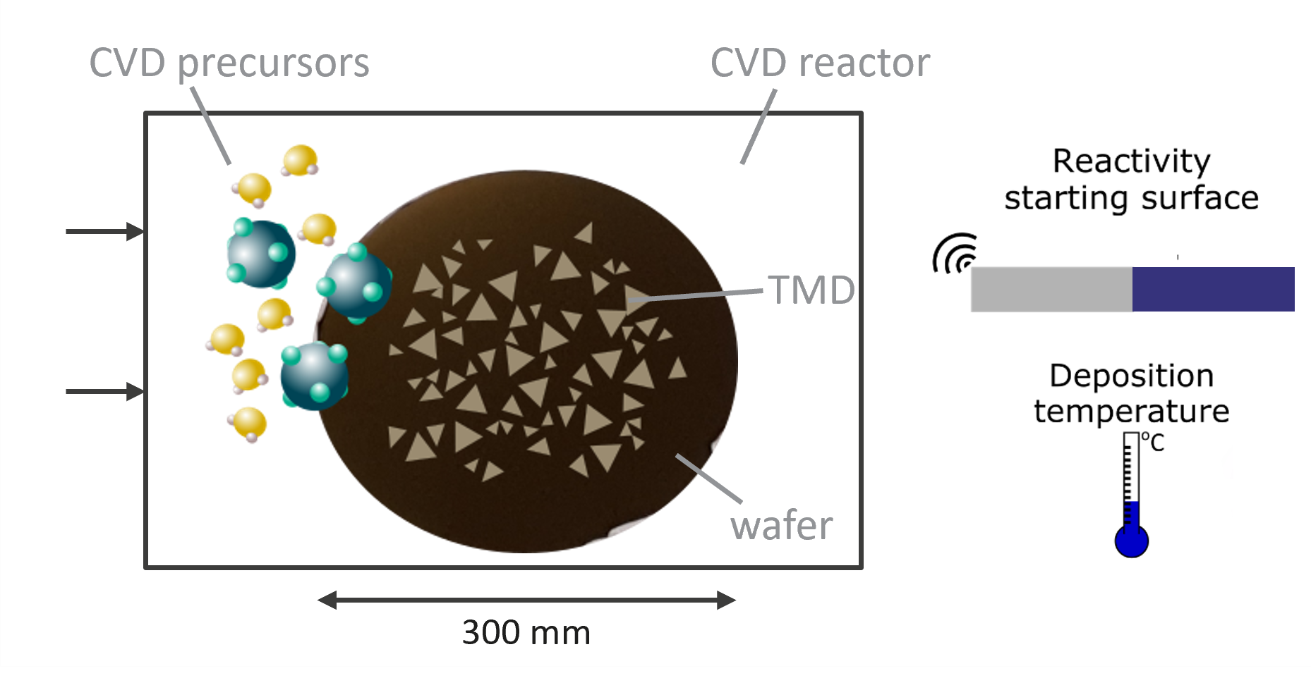
Therefore, this PhD research explores innovative selective deposition concepts to mitigate TMD crystal defects by controlling where a TMD material grows, and how these crystals orient and eventually coalesce. The approach is based on the intentional introduction of artificial nanoscale features on an amorphous starting surface. During this PhD research, you will embark on a journey to reveal how the geometry, chemical composition and critical (physical) dimensions of the design affect where TMD crystals nucleate and how they orient during the CVD process. You can propose various strategies to alter the chemical reactivity of starting surface by surface functionalization, and to introduce a relief or symmetry to a planar surface.
Your research will greatly benefit from the expertise and analytical methodologies that have been developed in the international and multidisciplinary 2D materials research team at imec [6,7,8].
- You will study the growth evolution of TMD crystals on various type of surfaces by complementary experimental characterization including scanning probe and electron microscopy and various types of surface sensitive spectroscopy.
- As such, you gain insight in the CVD precursor adsorption and diffusion.
- Ultimately, these observations can enable you to propose a growth mechanism.
- Based on that fundamental insight, you will leverage the design of the starting surface to tune the TMD crystal shape, orientation and defectivity in function of the envisioned device application, a high-performance planar field-effect transistor.
The PhD candidate is strongly encouraged to reflect on the considered research avenues by means of a comprehensive overview of the existing literature and analytical assessment. Depending on the personal interest, the candidate can explore the TMD adsorption and diffusion kinetics by either experimental means, or in combination with theory to understand better how to maximize selectivity towards the envisioned architecture. The candidate will work with state-of-the-art and industry-standard 300 mm CVD reactors, equipped with various transition metal and chalcogen precursors. This provides a unique perspective to explore the role of the CVD precursor chemistry on the TMD crystal growth mechanism. Lastly, plentiful opportunities arise for the candidate to further enrich personal and technical competences, for example through access to imec’s state-of-the-art clean room infrastructure and the imec academy development center, as well as research visit(s) to (academic) partners.
[1] Joyce, B. D. and Baldrey, J. A. (1962). “Selective Epitaxial Deposition of Silicon.” Nature, 195 (4840), 485–486.
[2] Filby J. D. and Nielsen S. (1967). “Single-crystal Films of Silicon on Insulators.” Br. J. Appl. Phys. 18 1357
[3] Klykov V. I., Sheftal N. N. and Hartmann E. (1979). “Artificial Epitaxy (Diataxy) of Silicon and Germanium.” Acta Physica Academiae Scientiarum Hungaricae, 47, 167–183
[4] Ly, T. H. et al. (2016). “Misorientation-angle-dependent Electrical Transport across Molybdenum Disulfide Grain Boundaries.” Nature Comm., 7, (10426)
[5] Kim, K.S., et al. (2023). “Non-epitaxial Single-crystal 2D Material Growth by Geometric Confinement.” Nature, 614, 88–94.
[6] Groven B., et al. (2017). “Plasma-Enhanced Atomic Layer Deposition of Two-Dimensional WS2 from WF6, H2 Plasma, and H2S.” Chem. Mater. 29 (7), 2927-2938
[7] Groven B., et al. (2018). “Two-Dimensional Crystal Grain Size Tuning in WS2 Atomic Layer Deposition: An Insight in the Nucleation Mechanism.” Chem. Mater. 29 (7), 2927-2938
[8] Shi Y., et al. (2021). “Engineering Wafer-Scale Epitaxial Two-Dimensional Materials through Sapphire Template Screening for Advanced High-Performance Nanoelectronics.” ACS Nano 15, 6, 9482-9494

Required background: Chemistry, Physics, Nanoscience and Nanotechnology, Materials Science and Engineering, Chemical Engineering
Type of work: 80% experimental, 10% theory, 10% literature
Supervisor: Annelies Delabie
Daily advisor: Benjamin Groven
The reference code for this position is 2025-049. Mention this reference code on your application form.
