A power delivery network is designed to provide power supply and reference voltage (i.e., VDD and VSS) to the active devices on the die most efficiently. Traditionally, it is realized as a network of low-resistive metal wires fabricated through back-end-of-line (BEOL) processing on the frontside of the wafer. The power delivery network shares this space with the signal network, i.e., the interconnects that are designed to transport the signal.
To deliver power from the package to the transistors, electrons traverse all 15-to-20 layers of the BEOL stack through metal wires and vias that get increasingly narrow (hence, more resistive) when approaching the transistors. On their way, they lose energy, resulting in a power delivery or IR drop when bringing the power down. When arriving closer to the transistor, i.e., at the standard cell level, the electrons end up in VDD and VSS power and ground rails organized in the Mint layer of the BEOL. These rails take up space at the boundary and between each standard cell. From here, they connect to the source and drain of each transistor through a middle-of-line interconnect network.
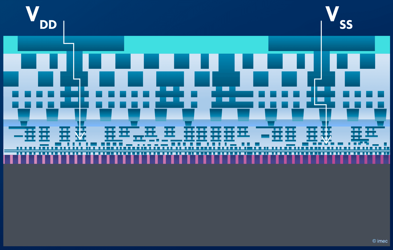
Figure 1 – Schematic representation of a traditional frontside power delivery network.
But with each new technology generation, this traditional BEOL architecture struggles to keep pace with the transistor scaling path. Today, the ‘power interconnects’ increasingly compete for space in the complex BEOL network and account for at least 20 percent of the routing resources. Also, the power and ground rails take up a considerably large area at the standard cell level, limiting further standard cell height scaling. At the system level, the power density and IR drop increase dramatically, challenging designers to maintain the 10 percent margin that is allowed for the power loss between the voltage regulator and the transistors.
Explore this 2023 research update about a DTCO study of backside power delivery options
Promises of a backside power delivery network
A backside power delivery network promises to address these issues. The idea is to decouple the power delivery network from the signal network by moving the entire power distribution network to the backside of the silicon wafer, which today serves only as a carrier. From there, it enables direct power delivery to the standard cells through wider, less resistive metal lines, without the electrons needing to travel through the complex BEOL stack. This approach promises to benefit the IR drop, improve the power delivery performance, reduce routing congestion in the BEOL, and when properly designed, allow for further standard cell height scaling. [1]
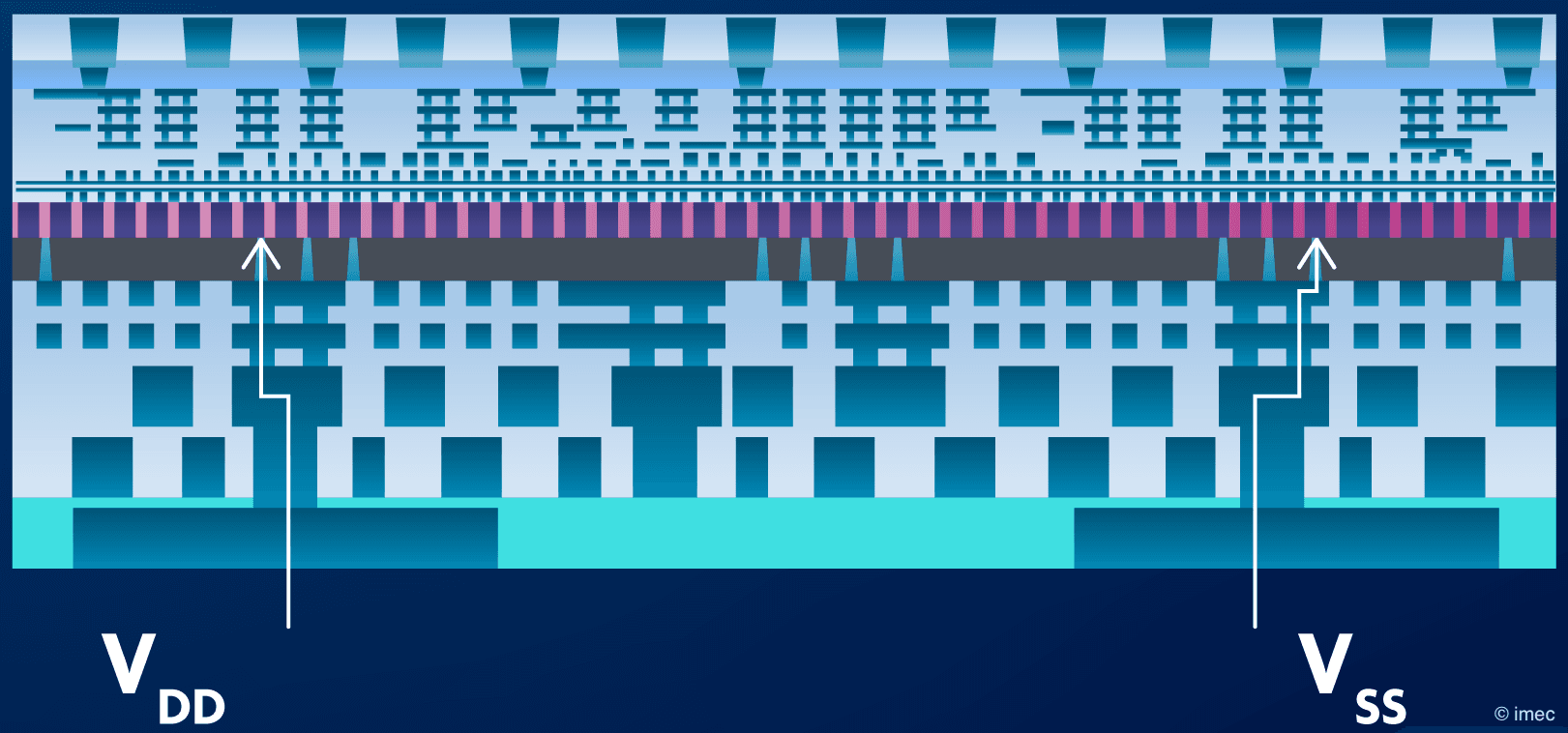
Figure 2 – A backside power delivery network allows for decoupling the power delivery from the signal network.
Buried power rail and nano-through-silicon-vias: key technology building blocks
Before detailing the process flow to fabricate a backside power delivery network, we introduce two technology enablers: buried power rail (BPR) and nano-through-silicon-vias (nTSVs).
BPR is a technology scaling booster that further scales standard cell height and reduces IR drop. It is a metal line construct buried below the transistors – partially within the Si substrate, partially within the shallow trench isolation oxide. It takes the role of the VDD and VSS power rails that have traditionally been implemented in the BEOL at the standard cell level. This historic move from BEOL to the front-end-of-line (FEOL) allows to reduce the number of Mint tracks, enabling a further shrinking of the standard cell. In addition, when designed perpendicularly to the standard cell, the rail’s size can be relaxed which further reduces the IR drop.
The potential of the BPRs can be fully exploited when combined with nTSVs, high-aspect-ratio vias processed in the thinned wafer’s backside. Together, they allow for delivering the power from the wafer’s backside to the active devices in the front-end in the most efficient way, i.e., with the largest gains in terms of IR drop reduction.
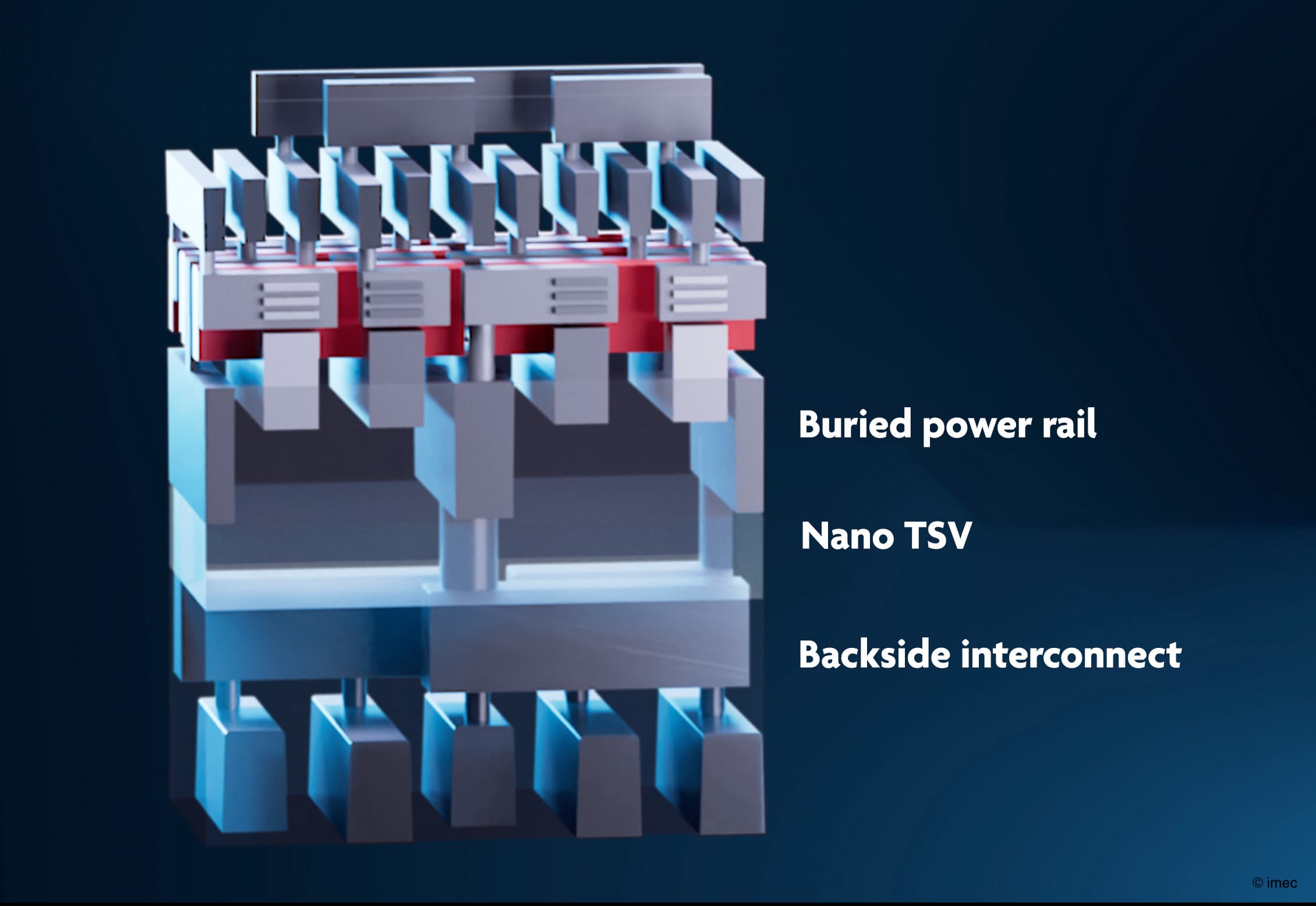
Figure 3 – Schematic representation of a backside power delivery network implementation where nanosheets connect to the wafer’s backside through BPRs and nTSVs.
Quantifying the promises of backside power delivery
At the 2019 IEDM conference, these promises have been quantified by imec research in collaboration with Arm [2]. Arm ran a simulation on one of their central processing units (CPUs) engineered with advanced design rules. They compared three ways to deliver the power: conventional frontside power delivery, frontside power delivery in combination with BPRs, and backside power delivery with nTSVs landing on BPRs. In terms of power delivery efficiency, the latter was the clear winner. On-chip power heat maps showed that BPRs with frontside power delivery could reduce the IR drop by ~1.7x compared to traditional frontside power delivery. But BPRs with backside power delivery did even better: they substantially reduced the IR drop by 7x.
Figure 4 – Comparing different power delivery approaches in terms of dynamic IR drop.
The overall process flow
Below, we unravel the process flow to make one specific implementation of a BSPDN, in which nTSVs – processed in an extremely thinned wafer backside – land on top of the BPRs. The devices, e.g., scaled FinFETs processed in the wafer’s frontside, connect to the backside of the wafer through the BPRs and nTSVs.
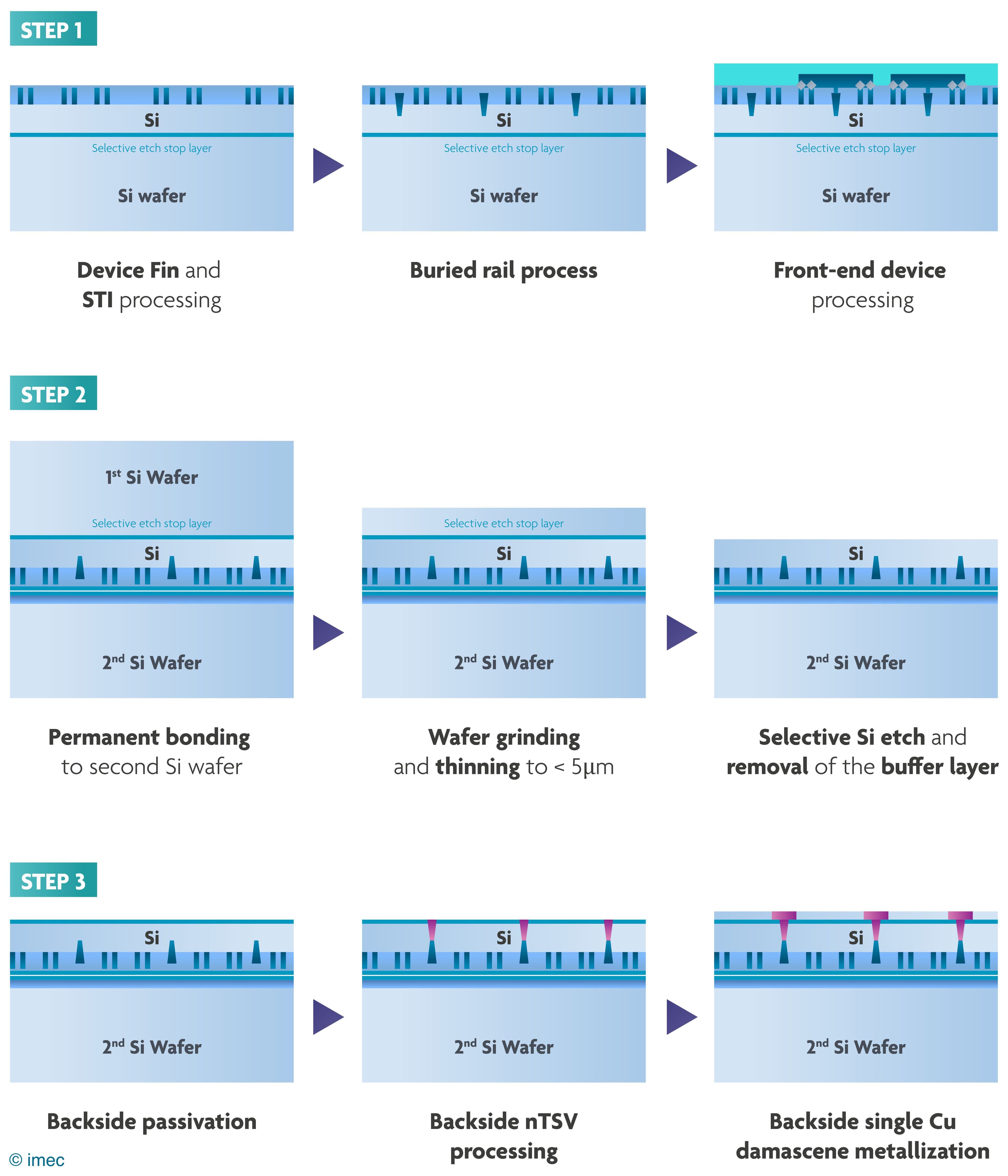
Figure 5 - Process flow for a backside power delivery network with BPRs connecting to nTSVs. For reasons of simplification, some details from step 1 have been omitted in steps 2 and 3, including the connection between BPR and the devices.
Step 1: frontside processing with buried rails
The process flow starts with growing a SiGe layer on top of a 300mm Si wafer. The SiGe layer later serves as an etch stop layer to end the wafer thinning (step 2). Next, a thin Si capping layer is grown on top of the SiGe layer: the starting point to fabricate the device and buried power rail. The buried power rails are defined after shallow trench isolation. The trenches, etched in the Si capping layer, are filled with oxide liner and metal, for example W or Ru. The resulting buried rails are typically ~30nm wide, at ~100nm pitch. The metal is then recessed and capped by a dielectric. Processing of the devices (in this case, scaled FinFETs) is completed after BPR implementation, and the BPRs are connected to the transistors source/drain region through the VBPR via and the M0A line. Cu metallization completes the frontside processing.
Step 2: wafer-to-wafer bonding and wafer thinning
The wafer containing the devices and BPRs is flipped over, and the ‘active’ frontside is bonded to a blanket carrier wafer. This is accomplished using SiCN-to-SiCN dielectric fusion bonding at room temperature, followed by a post-bond anneal at 250°C. Then, the backside of the first wafer can be thinned to where the SiGe etch stop is located. Thinning is enabled by a combination of sequentially backside grinding, chemical mechanical polishing (CMP), and dry and wet etch steps. The SiGe layer is removed in the next step, and the wafer is ready for nTSV processing.
Step 3: nTSV processing and connection to BPRs
After depositing a backside passivation layer, the nTSVs are patterned from the wafer backside by a through-Si alignment lithography process. nTSVs are etched through the Si (which is several 100nm deep) and land on the tip of the BPR. Next, the nTSVs are filled with oxide liner and metal (W). In this specific implementation, they are integrated at 200nm pitch without consuming any area of the standard cell. The flow is completed by processing one or more backside metal layers, electrically connecting the backside of the wafer to the BPR in the frontside via the nTSVs.
A closer look at the critical process steps
Implementing a backside power delivery network adds new steps to chip fabrication. Over the last few years, imec has demonstrated various critical technology building blocks, gradually addressing the challenges of the novel production steps. [3,4,5]
BPR: introducing metal in the front-end-of-line
In the proposed fabrication flow, buried power rails are implemented in the FEOL, before device processing. This implementation means the metal rail is subject to the high-temperature process steps applied during subsequent device manufacturing. For chip manufacturers, this might seem as disruptive as bringing Cu into the BEOL several decades ago. Therefore, the choice of metal used to make the BPR is crucial. Imec could successfully demonstrate the integration of buried power rails made of refractory metals – metallic elements like Ru or W that are highly resistant to heat. Keeping the metal rail en-capped during subsequent FEOL processing was an additional measure to avoid contamination of the front-end.
Imec believes that using nTSVs in combination with BPRs is a very promising implementation scheme in terms of scalability and performance. Other implementations of a backside power delivery network exist as well, each trading off power delivery performance, standard cell area consumption and front-end-off-line complexity.
Wafer thinning: minimizing thickness variation
Extreme wafer thinning to a few 100nm of Si is required to expose the nTSVs and minimize their resistivity (and hence, IR drop). This severely restricts the allowed thickness variation, which may be induced during the different wafer thinning steps. Imec collaborates with several partners to improve the chemistries used for etching. The final wet etch, for example, enables a highly selective soft-landing process stopping on the SiGe layer. In the final step of the thinning process, the SiGe etch stop layer is removed in a dedicated chemistry where very high selectivity to Si is required. This way, the Si capping layer can be exposed with a total thickness variation below 40nm.
Another concern is the thermal impact on the device self-heating due to the extreme thinning of the (otherwise heat-dissipating) Si substrate. Preliminary modeling work indicates that the self-heating effect can, to a large extent, be countered by the metal lines in the wafer’s backside, which provide additional lateral thermal spreading. More detailed thermal simulations are currently ongoing to gain more insights. [6]
Wafer bonding: precise nTSV/BPR alignment
The wafer bonding step inherently distorts the first ‘active’ wafer. This distortion challenges the lithography step needed to pattern the nTSVs on the wafer’s backside. More specifically, it challenges the precision with which the nTSVs need to be aligned to the bottom BPR layer. Since we are dealing with features that are of standard cell dimensions, the overlay requirement should be better than 10nm. Conventional lithography alignment can, however, not sufficiently compensate for the wafer distortion. Fortunately, advances in wafer-to-wafer bonding allow for a significant reduction in alignment errors and distortion values. In addition, by using advanced lithography correction techniques, the overlay error of the nTSV lithography with respect to the BPR structures can be reduced to less than 10nm.
No degradation of the device performance
One important question remains: are the newly added process steps, such as BPR integration, wafer thinning, and nTSV processing, impacting the electrical performance of the devices fabricated in the front-end?
To answer this question, imec recently built a test vehicle using the fabrication flow and the improved process steps described above. In this test vehicle, scaled FinFETs connect with tight overlay control to the wafer’s backside through 320nm deep nTSVs landing on BPRs. The BPRs also connect to the frontside metallization through the M0A layer and V0 via. This frontside connection, among others, allowed researchers to assess the electrical performance of the devices before and after backside processing. With this test vehicle, imec showed that FinFET performance was not degraded by BPR implementation and backside processing, provided that an anneal step is performed at the end to get optimal device properties. [4]
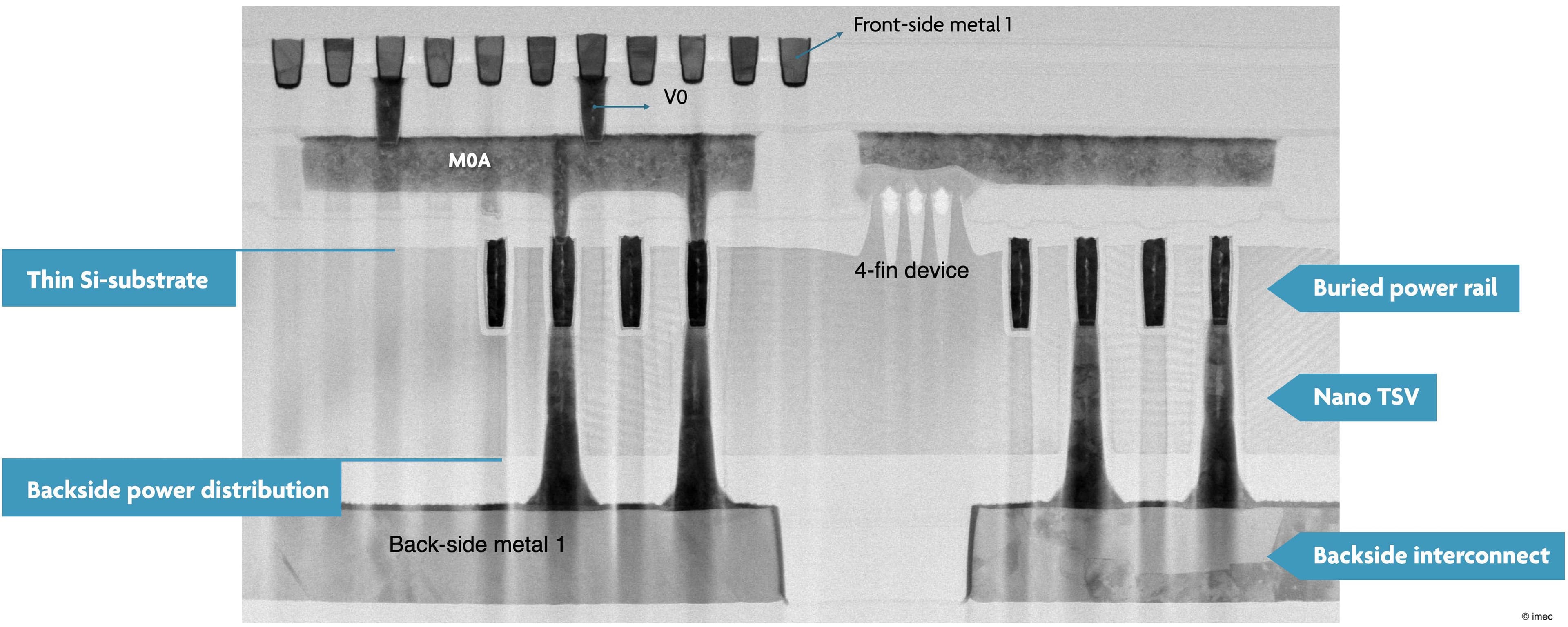
Figure 6 – TEM image showing scaled FinFETs connected to the wafer’s backside and frontside.
Application space: advanced logic ICs and extension to 3D-SOCs
Some chip manufacturers have publicly announced introducing backside power delivery networks in logic ICs of the 2nm and beyond technology node. This is when nanosheet transistors are making inroads. However, the novel routing technology can be used for a broad range of transistor architectures. Imec’s roadmap foresees its introduction in advanced technology nodes, with nanosheet transistors in 6T standard cells. The combination with BPR will then help push standard cell heights below 6T.
But the application domain extends beyond just 2D single-chip ICs: it also holds promises for the performance improvement of 3D systems-on-chip (3D SOCs). Imagine 3D-SOC implementation where some or all memory macros are placed in a top die while logic is placed on a bottom die. On the technology side, this can be realized by bonding the active frontside of the ‘logic wafer’ to the active frontside of the ‘memory wafer’. In this configuration, the original backsides of both wafers now reside on the outside of the 3D-SOC system. We can now think of exploiting the ‘free’ backside of the ‘logic wafer’ to deliver the power to the power-hungry core logic circuits. This can be accomplished in the same way as proposed for 2D SOCs. The main difference: the original dummy blanket wafer – earlier introduced to enable the wafer thinning – is now replaced by a second, active wafer (in this case, a memory wafer).

Figure 7 – Schematic representation of a 3D-SOC with backside power delivery implementation.
Although such a design is yet to be implemented experimentally, first assessments from the IR drop perspective are very encouraging. The proposed solution was validated on a memory-on-logic partitioned design using an advanced node research process design kit (PDK). Implementing a backside-power delivery network with nTSVs and BPRs showed promising results: 81 percent and 77 percent average and peak IR drop reduction for the bottom die compared to conventional frontside power delivery. This makes backside power delivery ideal for 3D IC power delivery in advanced CMOS nodes. [7]
For both 2D and 3D designs, the concept of exploiting the wafer’s free backside can potentially be expanded to other functions by adding specific devices in the backside, such as I/Os or ESD devices. Imec, for example, combined backside processing with implementing a 2.5D (i.e., pillar-like) metal-insulator-metal capacitor (MIMCAP), which serves as a decoupling capacitor. The 2.5D MIMPCAP boosts capacitance density with a factor of 4 to 5, allowing a further improvement of the IR drop. The results were derived from an IR drop modeling framework calibrated with experimental data. [8]
To provide academia and industry early access to the most advanced technology nodes and acquaint them with the most recent technology disruptions such as wafer backside technology, imec launched its open PDK, embedded in EDA tool suites. Find out more.
Summary
Future chips may well break the tradition of delivering power through the frontside. A backside power delivery network with backside metals, buried power rails, and nTSVs has shown clear advantages in reducing the IR drop, releasing the BEOL routing strain, and improving standard cell height scaling. The critical process steps, including BPR integration, wafer bonding, wafer thinning, and nTSV processing, are gradually being improved, as such preparing the new routing technology to introduce in advanced logic technology nodes and future 3D SOCs.
This article was originally published in Chip Scale Review (pp. 41-48).
References
[1] B. Cline et al., ‘Power from below: buried interconnects will help save Moore's Law,’ in IEEE Spectrum, vol. 58, no. 9, pp. 46-51, September 2021, doi: 10.1109/MSPEC.2021.9531012
[2] ‘Arm shows backside power delivery as path to further Moore’s Law’, IEEE Spectrum, 2019
[3] A. Veloso et al., ‘Enabling logic with backside connectivity via n-TSVs and its potential as a scaling booster’, 2021 Symposium on VLSI Technology, 2021, pp. 1-2
[4] A. Veloso et al., ‘Scaled FinFETs connected by using both wafer sides for routing via buried power rails,’ 2022 IEEE Symposium on VLSI Technology and Circuits, 2022, pp. 284-285, doi: 10.1109/VLSITechnologyandCir46769.2022.9830177
[5] A. Jourdain et al., ‘Buried power rails and nano-scale TSV: technology boosters for backside power delivery network and 3D heterogeneous integration," 2022 IEEE 72nd Electronic Components and Technology Conference (ECTC), 2022, pp. 1531-1538, doi: 10.1109/ECTC51906.2022.00244
[6] H. Oprins et al., ‘Package level thermal analysis of backside power delivery network (BS-PDN) configurations’, 21st IEEE Intersociety Conference on Thermal and Thermomechanical Phenomena in Electronic Systems (ITherm 2022)
[7] G. Sisto et al., ‘IR-drop analysis of hybrid bonded 3D-ICs with backside power delivery and μ- & n- TSVs,’ 2021 IEEE International Interconnect Technology Conference (IITC), 2021, pp. 1-3, doi: 10.1109/IITC51362.2021.9537541
[8] R. Chen et al., 'Backside PDN and 2.5D MIMCAP to double boost 2D and 3D ICs IR-drop beyond 2nm node,' 2022 IEEE Symposium on VLSI Technology and Circuits (VLSI Technology and Circuits), 2022, pp. 429-430, doi: 10.1109/VLSITechnologyandCir46769.2022.9830328

Naoto Horiguchi is the Director of CMOS Device Technology at imec. He obtained a degree in Applied Physics in 1992 from the Tokyo University, Japan. He has worked in Fujitsu and the University of California Santa Barbara, where he was involved in developing devices using semiconductor nanostructures and advanced CMOS. He has been with imec since 2006, where he is engaged in advanced CMOS device R&D together with worldwide industrial partners, universities, and research institutes. His current focus is on CMOS device scaling down to the 1nm technology node and beyond.

Eric Beyne is a senior fellow, VP of R&D, and program director of 3D system integration at imec in Leuven, Belgium. He obtained a degree in electrical engineering in 1983 and a Ph.D. in Applied Sciences in 1990, both from the KU Leuven, Belgium. He has been with imec since 1986, working on advanced packaging and interconnect technologies.
More about these topics:
Published on:
25 November 2022


