Advancing the development of monolithic CFETs for adoption in the logic technology roadmap
Complementary FET (CFET) device architectures are expected to succeed gate-all-around (GAA) nanosheet transistors in the logic technology roadmap. In a CFET device, n- and pMOS transistors are stacked on top of each other, removing the n-p separation from standard cell height considerations for the first time. As such, CFET device architectures have the potential to substantially shrink logic standard cell sizes, provided they can be combined with advanced technologies for contacting and powering the transistors.
Of all possible integration flows, monolithic CFET (mCFET) is considered the least disruptive – offering the fastest path to CFET introduction at industry-relevant dimensions. With monolithic integration, the vertical device structure with common top and bottom gates is patterned and processed in a single sequence of process steps.
The vertical stacking of layers brings along several challenges, and CFET-specific modules are needed to enable vertical isolation in critical parts of the stack cross-section. An example is the middle dielectric isolation (MDI) module, providing isolation between the top and bottom gates [1]. This allows different threshold voltages to be set for the top and bottom devices.
In recent years, considerable progress has been made in demonstrating the critical building blocks for a 300mm mCFET integration flow. At VLSI 2024, imec researchers reported on a mCFET device with MDI module, compatible with an inner spacer – a nanosheet-specific feature that isolates the gate from the source/drain (S/D) [2]. At IEDM 2024, imec experimentally demonstrated a functional mCFET with direct backside contact to the S/D of the bottom pMOS device [3].
Imec anticipates the introduction of the mCFET device architecture in the A7 node of the logic technology roadmap, when mCFET takes over from the outer wall forksheet. The latter is envisioned to extend the nanosheet-based logic roadmap into the A10 node, in anticipation of the mCFET being ready for mass production.
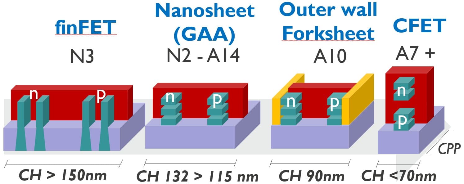
Figure 1 - Imec’s logic technology roadmap, showing the extension of the nanosheet era from 2nm to A10 node with the outer wall forksheet, before transitioning to CFET for A7 and beyond.
Extendibility of mCFET to further nodes: an industry concern
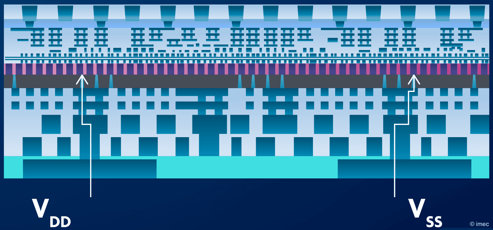
At circuit level, imec proposed the double-row CFET architecture as the most optimal way to integrate mCFETs into an A7 standard cell [4]. A double-row CFET standard cell contains two rows of stacked devices with a shared vertical signal via in between, and ‘VSS’ power walls at the cell boundary. At IEDM 2024, imec showed through a design-technology co-optimization (DTCO) study how this double-row CFET architecture offers the best trade-off between manufacturability and area efficiency for the A7 technology node.
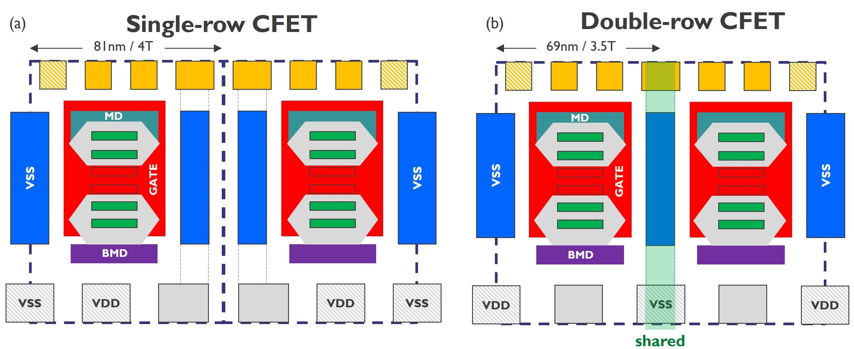
Figure 2 – Conceptual representation of (a) a single-row and (b) a double-row CFET.
However, industry has always been reluctant to switch to a new device architecture as this entails huge tool investments and additional risks. For the transition to be successful, it is important that the new architecture can be used across different nodes.
The imec researchers therefore continued their DTCO study to investigate the scalability of the double-row mCFET into subsequent technology nodes.
To evaluate power-performance-area (PPA) metrics at circuit level, the behavior of a 15-stage ring oscillator (i.e., a RO containing 15 mCFET-based inverters) was simulated. The RO was implemented using increasingly smaller standard cell layouts, complying to A7, A5, and A3 node specifications. To support scalability, the RO’s performance must be maintained across nodes, under a constrained power density budget. A key metric for the performance evaluation is the RO’s frequency, expressed as the ratio of the effective drive current and the effective capacitance.
Parasitic capacitance optimization, forksheet architecture, M0 power rail and hybrid channels: critical performance boosters
With shrinking standard cell dimensions, the sheet widths of the individual CFET channels reduce as well, lowering the effective drive current and enhancing the parasitic capacitance. Performance boosters will therefore be needed to balance these parameters and keep iso performance across nodes, while limiting the rise in power density. The DTCO study, presented at 2025 IEDM, reveals which boosters are needed for each node to support the aggressive area scaling targets [5].
For the A7 node, an RO performance comparable to a N2 nanosheet node can be obtained by further minimizing the gate parasitic capacitance. This can be achieved by reducing the gate area and the conductor area facing the gate. Optionally, moving the power wall of the double-row CFET to the middle of line (MOL) – as such ending up with an M0 power rail – can give an additional benefit.
Scaling into the A5 node requires the introduction of an outer wall forksheet device architecture. Until now, the forksheet architecture was put forward as an extension of nanosheet-type devices [6], but its architecture is fully compatible with CFET designs. The wall last approach – characteristic of the outer wall forksheet flavor – is of interest as it enhances channel stress, as such boosting the drive current of the CFET device. The smaller gate extension – allowed by the forksheet’s shared n-n or p-p wall – reduces the gate parasitic capacitance. Even more benefits are achieved by implementing an omega-shaped gate, which wraps the channel more effectively.
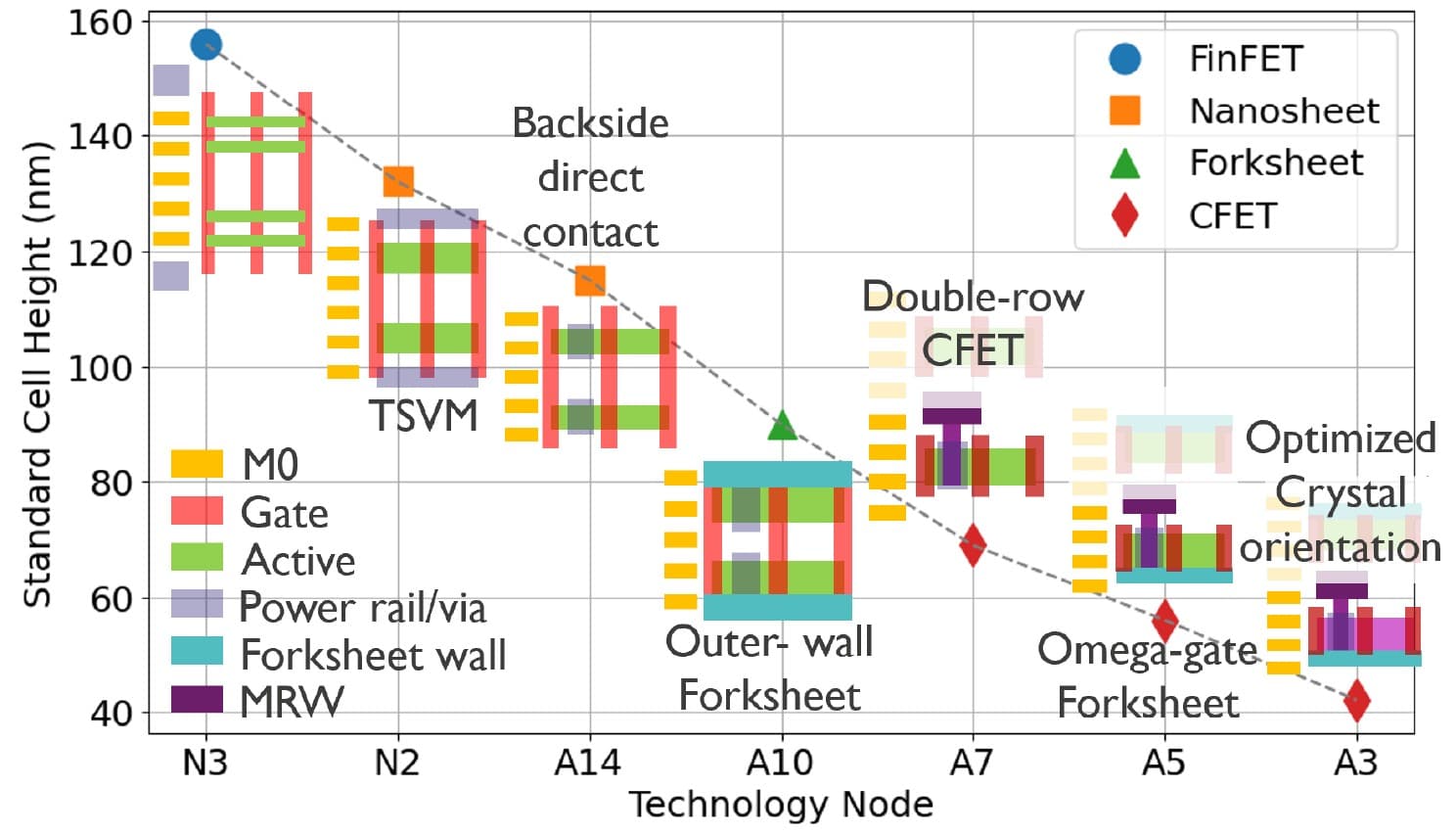
Figure 3 – Standard cell height scaling from FinFET to CFET. Double-row CFET scaling to A3 requires omega-gate forksheet and device current boosters (as presented at IEDM 2025).
The A3 node requires an extra performance booster in addition to the omega-gate outer wall forksheet and M0 power rail. The effective drive current can be further enhanced by introducing hybrid channel orientations. Tuning the channel orientation impacts the mobility of the charge carriers, the most optimal orientation being different for n and p-type devices. Note that the optimal choice also depends on whether strain is introduced in the channel (and how much). The imec team evaluated various channel orientations, with the most optimal combination enhancing the drive current by up to 20%. The associated increase in power density can be compensated for by balancing the channel width.
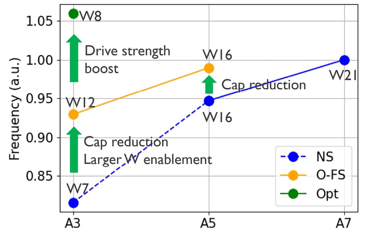
Figure 4 – Performance of the RO when scaling from A7 to A3, and the impact of performance boosters (as presented at IEDM 2025).
Embedded MDI module opens doors to hybrid channel orientations in an A3 mCFET process flow
At IEDM 2025, imec has experimentally demonstrated the key module that allows integrating channels with different orientations for the top nMOS and bottom pMOS devices in a mCFET process flow: the embedded MDI module [7].
The process flow for creating the eMDI starts with a carrier and a donor wafer on which the CFET-specific stacks of Si and sacrificial SiGe layers are grown epitaxially, for the bottom and top channels respectively. These epitaxial stacks are then recombined using wafer fusion bonding. The SiCN bonding dielectric becomes the embedded MDI single film of the mCFET device architecture, isolating the bottom and top parts. After these steps, processing of the mCFET is completed using the conventional mCFET flow, including nanosheet patterning, Si fin reveal, gate and inner spacer formation, bottom and top S/D epitaxy, and replacement metal gate.
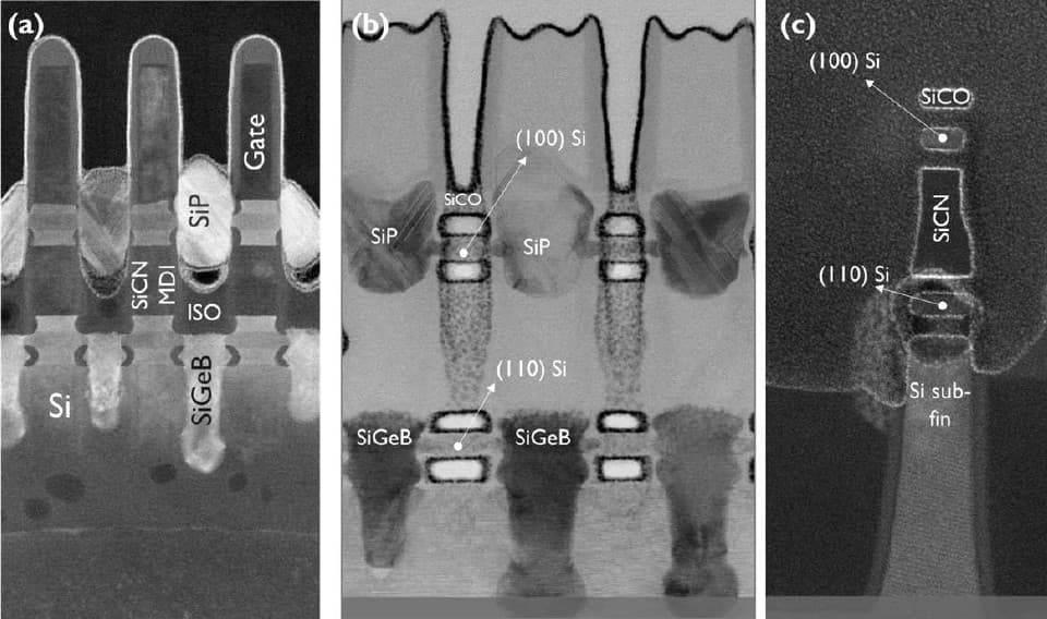
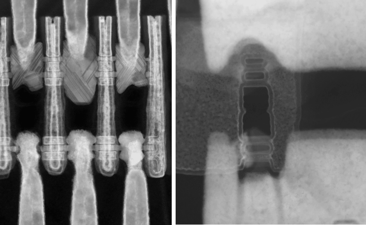
Figure 5 – TEM cross-sections of mCFET with eMDI module and top (100) Si channel and (110) bottom channel (as presented at IEDM 2025).
Imec successfully integrated this eMDI module in a full mCFET flow, and demonstrated functional top devices with various channel orientations: (100) Si top nFETs, (100) and (110) Si top pFETs. The top devices were fabricated with frontside connectivity.
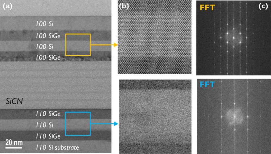
Figure 6 – SiCN MDI layer transfer with hybrid nanosheet channels featuring top (100) Si orientation and bottom (110) Si orientation: (a) TEM and (b) high-resolution TEM cross-sections and (c) Fast Fourier Transform confirming the 2 different crystal orientations (as presented at IEDM 2025).
The integration flow was then extended with direct backside contacting to the mCFET bottom device. The imec CFET team demonstrated functional mCFET devices with integrated eMDI module, (100) Si top nFET connected from the frontside, and (110) Si pFET with direct backside contact.
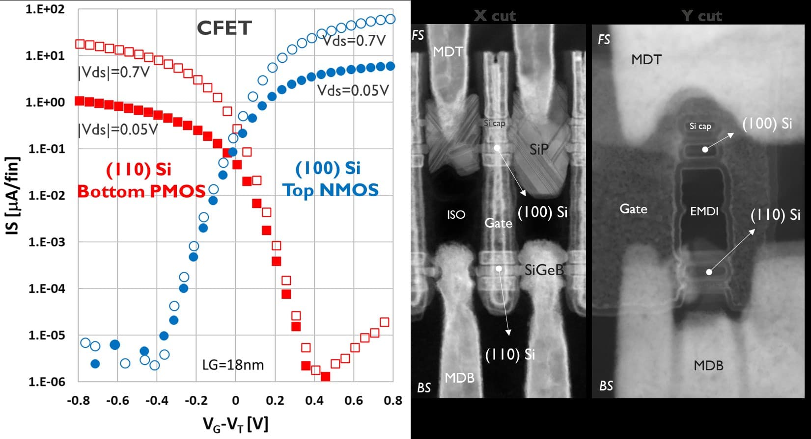
Figure 7 – (Left) Id/Vg curves and (right) TEM cross sections of mCFET with eMDI module, (100) Si top nFET, and backside contacted (110) Si bottom pFET.
Benefits of eMDI: heterogeneous channels, simplified MDI process flow, simpler Si/SiGe epi growth, more stacked Si channels
The eMDI module has several benefits compared to an earlier flavor of the MDI module, referred to by imec as the replacement MDI or rMDI [1]. With rMDI, the active Si/SiGe epi stack is turned into one tall Si/SiGe1/SiGe2 multilayer stack. Later in the process flow, the sacrificial SiGe1 layers are replaced with the gate’s work function metals, and the Ge-rich SiGe2 layers are converted into the MDI dielectric.
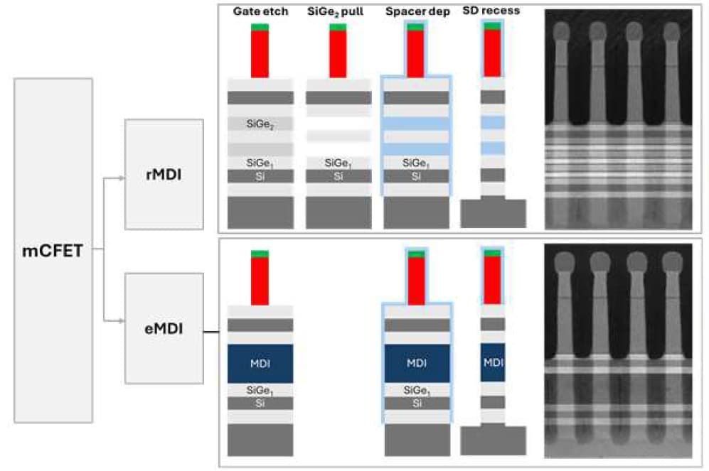
Figure 8 – Comparison of the eMDI and rMDI integration approaches (as presented at IEDM 2025).
The main difference between both approaches is the initial substrate engineering. In the eMDI case, mCFET processing starts from an advanced, bonded substrate with the MDI module already embedded. The use of separate wafers for growing the n- and pMOS active epi stacks prior to the bonding for the first time allows to integrate heterogeneous channels, optimized for maximum n- and pMOS performance. These can be channels with different orientations – as demonstrated in this study – but also, channels with different strain, and even different materials for n and p.
Other advantages include reduced process complexity and simpler epi steps: eMDI avoids the deposition of the complex Si/SiGe1/SiGe2 multilayer stack and the replacement of the dummy SiGe2 layers with a dielectric. Also, by growing the epi stacks on two separate wafers, more Si channels can be included before layer relaxation is reached during epi growth – increasing flexibility in design. The novel MDI module can be integrated into any mCFET baseline, with minor modifications to the mCFET flow.
Outlook: different channel materials, embedded bottom dielectric isolation module
Imec is currently optimizing the critical modules of the eMDI-based mCFET flow with different channel orientations. Future work will extend the proposed scheme to integrate different channel materials for n and p, i.e., Ge for pMOS and Si for nMOS.
In addition, the imec CFET team intends to use a similar ‘embedded’ approach to integrate the bottom dielectric isolation (BDI), a process module that is needed to isolate the S/D epi from the substrate. Using an eBDI approach relying on layer transfer by wafer bonding is expected to facilitate the integration of the backside connection, compared to today’s replacement BDI (rBDI) counterpart. In addition, the eBDI approach will allow more freedom of choice for the BDI material. One option is to use a high thermal conducting material, which may alleviate concerns about the thermal reliability of mCFETs.
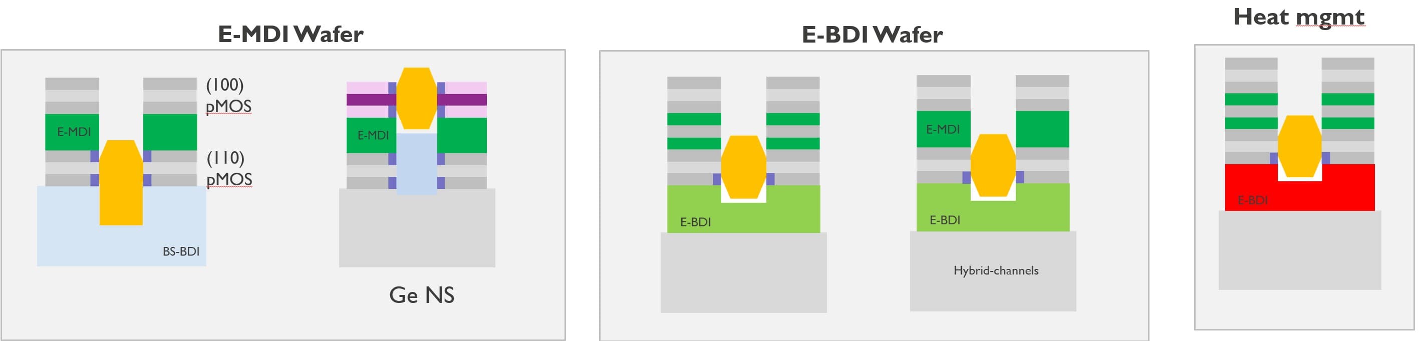
Figure 9 – Advanced substrate options for mCFET, with eMDI and eBDI module options.
Conclusion
Imec has identified through a DTCO study the performance boosters that are needed to support aggressive area scaling of mCFET device architectures across multiple technology nodes. While minimizing parasitic gate capacitance is essential for the A7 node, the A5 and A3 nodes will see the introduction of the outer wall forksheet with omega-shaped gate, and an M0 power rail. For A3, additionally introducing heterogeneous channels optimized for p- and nMOS separately will be crucial to maintain performance and power density at ultimately scaled standard cell dimensions. An eMDI module is the key enabling technology for integrating heterogeneous channels in a mCFET flow. This was demonstrated experimentally on mCFET devices with different channel orientations for nMOS and pMOS top devices.
This work has been enabled in part by the NanoIC pilot line. The acquisition and operation are jointly funded by the Chips Joint Undertaking, through the European Union’s Digital Europe (101183266) and Horizon Europe programs (101183277), as well as by the participating states Belgium (Flanders), France, Germany, Finland, Ireland and Romania. For more information, visit nanoic-project.eu.
This article was originally published in Semiconductor Digest.
Want to know more?
[1] ‘Towards a process flow for monolithic CFET transistor architectures,’ imec reading room;
[2] ‘Monolithic complementary field effect transistors (CFET) demonstrated using middle dielectric isolation and stacked contacts,’ S. Demuynck et al., VLSI 2024;
[3] ‘Monolithic-CFET with direct backside contact to source/drain and backside dielectric isolation,’ A. Vandooren et al., IEDM 2024;
[4] ‘Imec proposes double-row CFET for the A7 technology node,’ imec press release;
[5] ‘Multi-node scaling potential of monolithic CFET,’ S. Yang et al., IEDM 2025;
[6] ‘Outer wall forksheet to bridge nanosheet and CFET device architectures in the logic technology roadmap,’ imec reading room;
[7] ‘Hybrid channel monolithic-CFET with Si (110) pMOS and (100) nMOS,’ A. Vandooren et al., IEDM 2025.