Nearing a key inflection point...
The chip industry has never been eager to move to a new transistor architecture for the high-volume production of chips, as this brings along new complexities and investments. But recent public announcements by e.g. Samsung, Intel, TSMC and IBM show that we are at the eve of such a transition. From 2022 or 2023 onwards, these companies have accepted to gradually transition from ‘workhorse’ FinFET transistor architectures to nanosheet-like architectures for producing logic chips of the 3nm or 2nm technology generations.
In this article, you will learn about the main drivers behind this historic transition. In addition, we will introduce different generations of the nanosheet architecture family, including nanosheet, forksheet and CFET. For each of these nanosheet family members, we will review incremental benefits in view of further CMOS scaling and talk about critical process steps.
To provide academia and industry early access to the most advanced technology nodes and acquaint them with the most recent technology disruptions such as nanosheet devices, imec launched its open PDK, embedded in EDA tool suites. Find out more.
Why moving from FinFET to nanosheet?
Along the logic CMOS scaling path, the semiconductor community made considerable efforts to gradually reduce the dimensions of logic standard cells.
Schematic representation of a logic standard cell layout (CPP = contacted poly pitch, FP = fin pitch, MP = metal pitch; cell height = number of metal lines per cell x MP).
One way to do this is to reduce cell height – which is defined as the number of metal lines (or tracks) per cell times the metal pitch – by reducing the track. For the FinFET, new generations with ever smaller cell heights were realized by gradually reducing the number of fins within one standard cell from 3 to 2. This has enabled 7.5T and 6T standard cells, respectively. With 6T, for example, we mean that 6 metal lines fit in the range of the cell height. This evolution comes however at the expense of drive current and variability if fin dimension is kept. To compensate for the degradation of drive current and variability, fins were getting taller in the cell height scaling. Eventually, this trend could continue to 1 fin, enabling 5T standard cells.
In FinFET-based architectures, fin depopulation is required for standard cell scaling. With each generation, fins are getting taller, thinner and closer. This evolution decreases drive strength and increases variability.
However, further enhancing the drive current of 5T FinFET-based single-fin device architectures is extremely challenging. And this is where nanosheet architectures enter the scene. By vertically stacking nanosheet-shaped conduction channels in standard cells where only one fin is allowed, a larger effective channel width can be realized. This way, nanosheets can provide larger drive current per footprint than fins – a key benefit for further CMOS scaling. The nanosheet architecture also allows for a variable device width, which enables some flexibility in design: designers can now trade off enhanced drive current for reduced area and capacitance (smaller channel width tends to reduce parasitic capacitance between the sheets). Another notable advantage of a nanosheet over a FinFET architecture is its ‘gate-all-around’ structure: as the conduction channel is now completely surrounded by the high-k/metal gate, improved gate control over the channel is achieved for shorter channel lengths.
Critical nanosheet building blocks
Like the transition from planar MOSFETs to FinFETs, the transition from FinFETs to gate-all-around nanosheet transistors came along with new process integration challenges. Fortunately, the nanosheet can be considered a natural evolution of the FinFET, and therefore, many of the process modules developed and optimized for the FinFET could be re-used. This for certain has facilitated its adoption by industry. Nevertheless, we identify four key process steps in which the two architectures differ, and which have required specific innovations.
The first is that this architecture uses epitaxially-grown multilayers of Si and SiGe to define the device channel. The use of grown materials for the channel and the lattice mismatch between the two materials represent a departure from the traditional fabrication of CMOS devices. In this multilayer stack, SiGe serves as a sacrificial layer that is removed later on, during the channel release within the replacement metal gate steps. The whole multilayer stack is patterned in the form of a high-aspect ratio fin, which presents a challenge for maintaining a good nanosheet shape. At the 2017 IEDM conference, imec proposed a key optimization: implementing a shallow trench isolation (STI) liner and using a low thermal budget in the STI process steps were shown to suppress oxidation-induced fin deformation. This has resulted in better nanosheet shape control, which was found to improve device performance – DC (i.e., larger drive current) as well as AC (i.e., speed gain at constant power). Improved AC performance translated into a lower gate delay of a ring oscillator circuit – which was the first report of a real circuit fabricated with the new nanosheet process flow [1, 2, 3].
Second, as opposed to the FinFET, the nanosheet architecture requires an inner spacer – an additional dielectric that isolates the gate from the source/drain for reduced capacitance. During the inner spacer formation process step, the outer portions of the SiGe layers in the multilayer structure are recessed using a lateral etch process. This creates small cavities which are then filled with dielectric materials. Inner spacer integration is the most complex process module of the nanosheet process flow. It needs high etch selectivity and precise lateral etch control. The inner spacer integration challenge was addressed by several research teams worldwide, including imec [2].
Third, there is the nanosheet channel release – the step where the nanosheets are separated from each other. This release is realized by selectively etching away the SiGe part of the multilayer. This process step demands a highly selective etch, ideally leaving few Ge residues between the nanosheets and reducing Si roughness. Also, stiction control is needed to avoid that these tiny nanosheets attach to each other. Imec’s fundamental study of different etch process options – dry as well as wet – has contributed greatly to solving these issues.
And finally comes the replacement metal gate (RMG) integration step, including the deposition and patterning of the work function metal around and in between the nanosheet layers. In 2018, imec highlighted the importance of introducing a scalable work function metal, allowing for a reduced vertical space of the nanosheet stack. The team showed for example that reducing the spacer between two vertical nanosheets from 13nm to 7nm improved the AC performance with 10% - emphasizing the significance of scaling the RMG [4].
Optimizations for vertically stacked gate-all-around nanosheet transistors: (left) nanosheet shape control; (right) nanosheet vertical space reductional separation.
And then comes forksheet
The most elegant way to further increase DC performance is by enlarging the effective width of the channels. But in conventional nanosheet architectures, this becomes very difficult. The main showstopper is the large space margin that is needed in between n- and p-type devices, which makes a large effective nanosheet width difficult in scaled cell heights. This space is consumed by the work function metal patterning step. The forksheet device architecture can address this challenge. The forksheet was for the first time publicly proposed by imec for SRAM scaling in 2017 (IEDM 2017), and later on (IEDM 2019) as a logic standard cell scaling enabler [5, 6]. In this architecture, smaller n-p separation is enabled by introducing a dielectric wall in between n- and pMOS devices before gate patterning. Hardmask patterning for work function metal patterning can now be done on this dielectric wall, instead of at the bottom of the gate trench in the nanosheet case. And this allows a much tighter n-to-p spacing.
Consequently, the effective width of the channels – and hence, the drive current (DC performance) – can be further enhanced. Instead of maximizing the effective channel width, the smaller n-to-p space can alternatively be exploited to further scale the track height of the standard cell from 5T to 4T. This evolution needs to be complemented by innovations in the back-end- and middle-of-line, and by introducing scaling boosters (such as buried power rails or self-aligned gate contacts).
Simulations also predict a 10% AC performance gain for forksheet over nanosheet. The imec team could explain this speed improvement by a reduced (parasitic) Miller capacitance resulting from a smaller gate-drain overlap. The small Miller cap potentially enables more energy efficient devices.
From processing point of view, the forksheet architecture naturally evolves from the ‘basic’ nanosheet architecture. Key differentiators are the dielectric wall formation, and modified inner spacer, source/drain epitaxy and replacement metal gate steps. At VLSI 2021, imec for the first time presented electrical data of forksheet field-effect devices that were successfully integrated using the 300mm forksheet process flow. Dual work function metal gates could be integrated at 17nm spacing between the n- and pFETs – highlighting the key benefit of the forksheet architecture [7].
There was however still one concern over the electrostatics. Nanosheet architectures are touted for their gate-all-around structure, which largely improves the electrostatic control over the channel. With its tri-gated architecture in the form of a fork, forksheet seems to take a step back. However, in the experiments mentioned above, imec found a short channel control (SSSAT = 66-68mV) at 20nm gate length that was comparable to that of vertically stacked gate-all-around nanosheet devices that were co-integrated on the same wafer [8].
TEM image of co-integrated fork- and nanosheet FETs. For the forksheet n-and pFETs, a dual work function metal gate is integrated at 17nm n-p space.
CFETs to complete the nanosheet family on the longer term
A further maximization of the effective channel width is possible with the Complementary FET or CFET architecture, where n- and pMOS devices are stacked on top of each other. This moves the n-p separation to the vertical direction, as such removing n-p spacing from cell height considerations. The channel width can now be further enlarged, but the resulting area gain can also be used to push track heights to 4T and below [9, 10]. Simulations have demonstrated that CFETs can be beneficial for future logic as well as SRAM area scaling. In a CFET, channels can be made in the form of either a fin (n-fin on p-fin) or a nanosheet (n-sheet on p-sheet). In the latter configuration, CFETs complete the nanosheet device architecture family as the ultimate CMOS device architecture.
From FinFET to nanosheet to forksheet and finally to CFET.
From processing point of view, the CFET architecture is complex due to its nMOS-pMOS vertically stacked structure. Two possible integration schemes exist for the vertical integration: monolithic and sequential. Each of these flows comes with its own set of pros and cons. Imec contributes by developing modules and integration steps, and by quantifying the power-performance-area benefits and the complexity of each of the process flows.
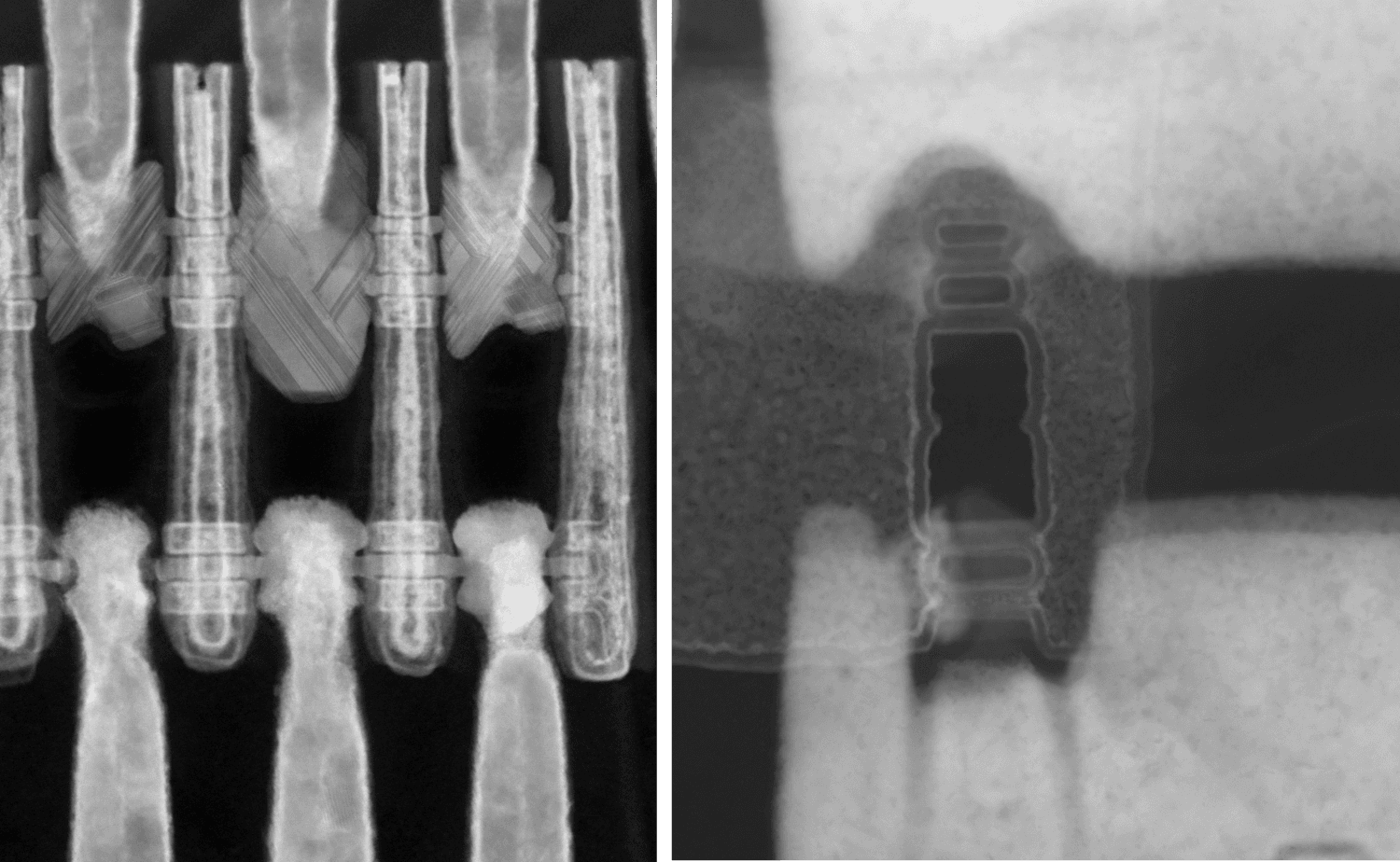
TEM pictures of a CFET processed with a monolithic fabrication flow. Left: CFET top device; right: CFET bottom device
Monolithic CFET: lower cost, but complex vertical integration
A monolithic CFET flow starts with the epitaxial growth of the bottom channel, followed by the deposition of an intermediate sacrificial layer and next, epitaxial growth of the top channel. The starting bottom and top channel configuration can be in the form of either a Si fin or a Si/SiGe multilayer stack when a nanosheet channel is targeted. In either case, the stacking approach results in very high aspect ratio vertical structures, which brings along critical challenges for further patterning the fin, gate, spacers and source/drain contacts. The replacement metal gate integration step, for example, is additionally complicated by the need for different work function metals for n and p. At VLSI 2020, imec was the first to demonstrate a monolithically integrated CFET architecture, realized by optimizing critical module steps [11].
Sequential CFET: hybrid channel materials, but challenged by wafer transfer
Sequential processing of CFETs consists of several blocks. First, the bottom tier device is processed up to the contacts. Next, a blanket semiconductor layer is created on top of this tier by wafer transfer, using a dielectric-to-dielectric wafer bonding technique. Then, the top tier device is integrated, and top and bottom gate are connected. The flow is completed with middle-of-line and back-end-of-line processing.
From integration point of view, this flow is simpler than the monolithic flow, as both bottom and top tier devices can be processed separately in a conventional ‘two-dimensional’ way. A notable advantage of the sequential integration flow is the flexibility in integrating different channel materials for n- and p-type devices (for example, Si for nMOS, SiGe or Ge for pMOS, or, ultimately, 2D materials such as WS2), offering a further performance advantage.
But as with all new processing schemes, there are some specific challenges that require special attention. The first relates to the thickness of the bonding dielectric oxide in between the two wafers. A too thick oxide comes at the expense of AC performance, as demonstrated by imec at VLSI 2020 [11]. On the other hand, making the oxide too thin holds a risk of creating bonding defects (in the form of voids). Imec made progress in developing a bonding-void-free thin bonding oxide process that balances both concerns.
Second, the wafer transfer approach comes with thermal budget constraints: the top tier process temperature needs to be reduced (to around 500°C) as to avoid any negative impact on the bottom tier devices. And this is a concern for both gate-stack reliability and dopant activation, which usually require thermal steps of the order of 900°C. Imec recently proposed solutions for both concerns. First, our team developed two new approaches for maintaining a good gate-stack reliability at lower processing temperatures: (1) a low-temperature hydrogen plasma treatment (to passivate defects in the Si-oxide interlayer) and (2) introduction of an interface dipole between the Si channel and the HfO2 gate dielectric (to offset the energy between HfO2 defect states and the charge carrier conduction band). Second, an innovative epitaxial growth process was developed that yields high dopant activation even at low growth temperatures – for both p- and nMOS devices [12, 13, 14, 15].
For both monolithic and sequential CFET integration schemes, imec continues to work towards improved module and integration steps, and to recommend best options to industry.
Conclusion
In this article, we reviewed the main benefits and challenges of introducing nanosheet-like transistor architectures for CMOS logic device scaling. Each new generation – enabled by nanosheet, forksheet and CFET – comes with a performance improvement (by optimizing effective channel width) and/or a further reduction of the logic standard cell height. From processing point of view, nanosheet architectures can be considered an evolutionary step over FinFET architectures. However, each of the different nanosheet architectures comes with specific integration challenges, for which imec continues to explore and assess solutions.
This article was (partly) published in EETimes.
Want to know more?
References:
[1] ‘Gate-all-around MOSFETs based on vertically stacked horizontal Si nanowires in a replacement metal gate process on bulk Si substrates’, H. Mertens et al, VLSI 2016
[2] ‘Vertically stacked gate-all-around Si nanowire transistors: Key Process Optimizations and Ring Oscillator Demonstration’, H. Mertens et al, IEDM 2017
[3] ‘Vertically Stacked Gate-All-Around Si Nanowire CMOS Transistors with Reduced Vertical Nanowires Separation, New Work Function Metal Gate Solutions, and DC/AC Performance Optimization’, R. Ritzenthaler et al, IEDM 2018
[4] ‘Power-performance trade-offs for Lateral NanoSheets on ultra-scaled standard cells’, M. Garcia Bardon, VLSI 2018
[5] ‘Stacked nanosheet fork architecture for SRAM design and device co-optimization toward 3nm’, P. Weckx et al, IEDM 2017
[6] ‘Novel forksheet device architecture as ultimate logic scaling device towards 2nm’, P. Weckx et al, IEDM 2019
[7] ‘Forksheet FETs for Advanced CMOS Scaling: Forksheet-Nanosheet Co-Integration and Dual Work Function Metal Gates at 17nm N-P Space’, H. Mertens et al, VLSI 2021
[8] “Comparison of Electrical Performance of Co-Integrated Forksheets and Nanosheets Transistors for the 2nm Technological Node and Beyond”, R. Ritzenthaler et al, IEDM 2021
[9] ‘The Complementary FET (CFET) for CMOS scaling beyond N3’, J. Ryckaert et al, VLSI 2018
[10] ‘Device-, Circuit- & Block-level evaluation of CFET in a 4 track library’ P. Schuddinck et al, VLSI 2019
[11] ‘First Monolithic Integration of 3D Complementary FET (CFET) on 300mm Wafers’, S. Subramanian et al, VLSI 2020
[12] ‘BTI Reliability Improvement Strategies in Low Thermal Budget Gate Stacks for 3D Sequential Integration’, J. Franco et al, IEDM 2018
[13] ‘Atomic Hydrogen Exposure to Enable High-Quality Low-Temperature SiO2 with Excellent pMOS NBTI Reliability Compatible with 3D Sequential Tier Stacking’, J. Franco et al, IEDM 2020
[14] ‘Contact Resistivity of Highly Doped Si:P, Si:As and Si:P:As Epi layers for Source/Drain Epitaxy’, E. Rosseel et al, ESC PRiME 2020
[15] ‘Very Low Temperature Epitaxy of Group-IV Semiconductors for use in FinFET, Stacked Nanowires and Monolithic 3D Integration’, C. Porret et al, ESC Journal of Solid State Science and Technology 2019
Further reading on nanosheets:
- ‘Imec reports first electrical demonstration of integrated forksheet devices to extend nanosheets beyond 2nm technology node’, imec press release
- ‘A view on the logic technology roadmap: advancing the front-end, back-end and middle-of-line towards the 1nm technology generation’, imec reading room;
- ‘Logic technology scaling options for 2nm and beyond’, imec reading room;
- ‘A novel approach for improving gate-stack reliability’, imec reading room.
If you would like to receive more info on this topic, fill in our contact form.

Naoto Horiguchi is the Director of CMOS Device Technology at imec. He obtained a degree in Applied Physics in 1992 from the Tokyo University, Japan. He has worked in Fujitsu and the University of California Santa Barbara, where he was involved in developing devices using semiconductor nanostructures and advanced CMOS. He has been with imec since 2006, where he is engaged in advanced CMOS device R&D together with worldwide industrial partners, universities, and research institutes. His current focus is on CMOS device scaling down to the 1nm technology node and beyond.
More about these topics:
Published on:
11 February 2022


