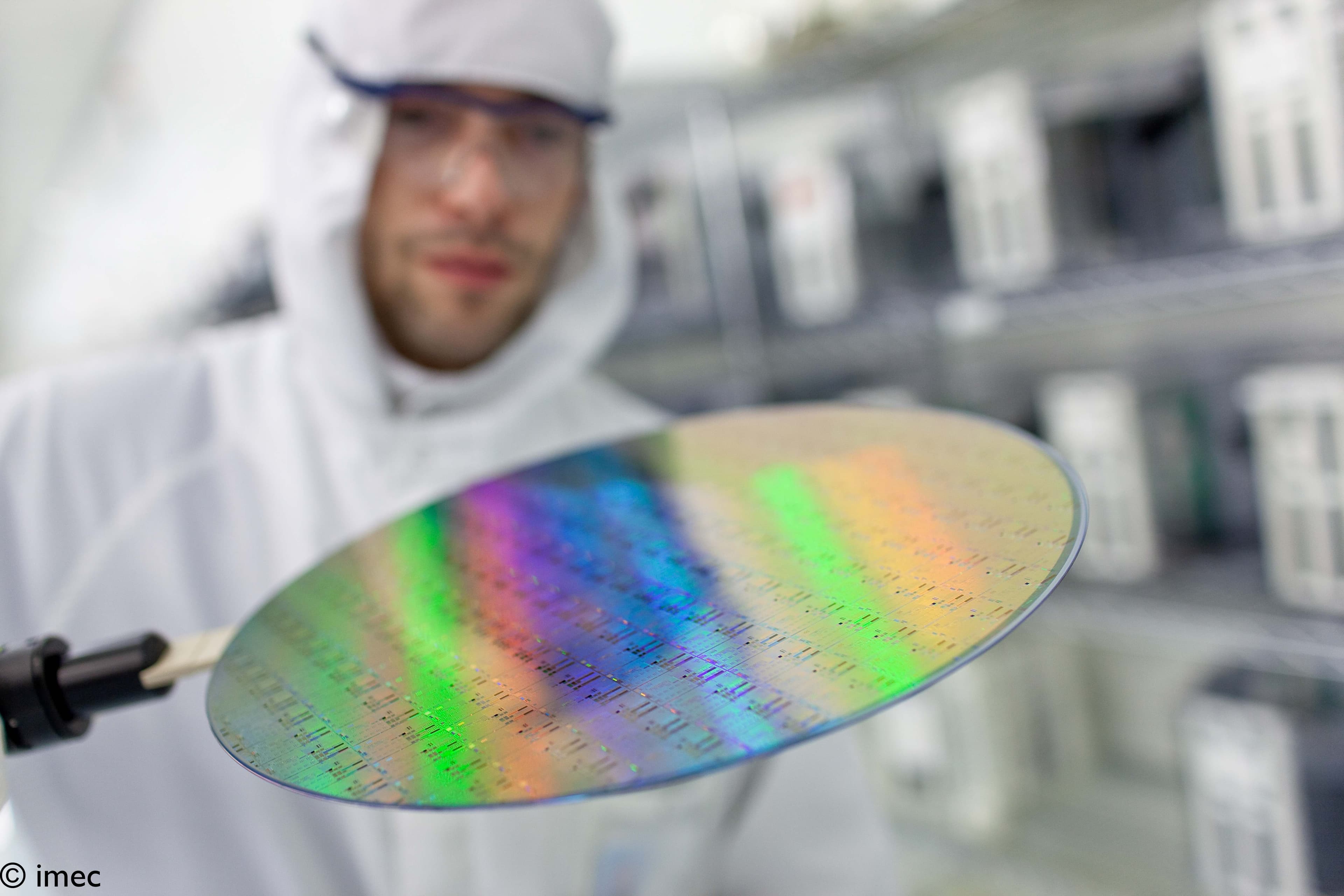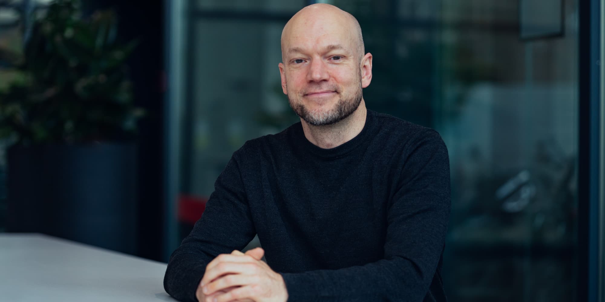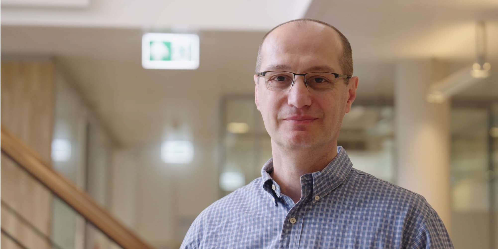
For Wilfried Vandervorst, advanced semiconductor technology is only as strong as the ability to measure, understand, and control it. As a senior imec fellow and professor emeritus at KU Leuven, Wilfried has helped shape the field of semiconductor metrology for more than four decades.
Metrology (and the science of measurement) is essential to chip innovation. It allows researchers and manufacturers to see what is happening inside increasingly small and complex semiconductor structures, from material composition and dopant profiles to defects, interfaces, and electrical behavior. Wilfried’s career has been dedicated to developing, improving and applying those measurement techniques at the limits of what is physically possible.
Making the invisible measurable
Wilfried received his MSc degree in electronic engineering from KU Leuven in 1977 and his PhD in Applied Physics from the same university in 1983. He worked at Bell Northern Research in Ottawa, Canada, as a consultant in materials characterization, before joining imec in 1984. He would become director of the department dealing with materials characterization. Since 1990, he has also held an appointment at KU Leuven’s physics department, teaching materials characterization and supervising PhD students.
In 2001, after an international peer review, he was elected imec fellow for his outstanding scientific achievements in semiconductor metrology. In 2013, he became imec senior fellow.
Wilfried’s work focused on developing and applying advanced metrology with the aim of providing fundamental insight into material interactions within semiconductor technology. That includes nanoscale materials characterization, secondary ion mass spectrometry, scanning probe microscopy, dopant profiling, ion beam analysis, and techniques that make it possible to study extremely small semiconductor structures in three dimensions, such as atom probe tomography.
From lab technique to semiconductor roadmap
Many metrology techniques that once belonged mainly in specialized labs are now essential to semiconductor research and manufacturing. Wilfried’s work has helped bring that level of measurement insight closer to the technology roadmap.
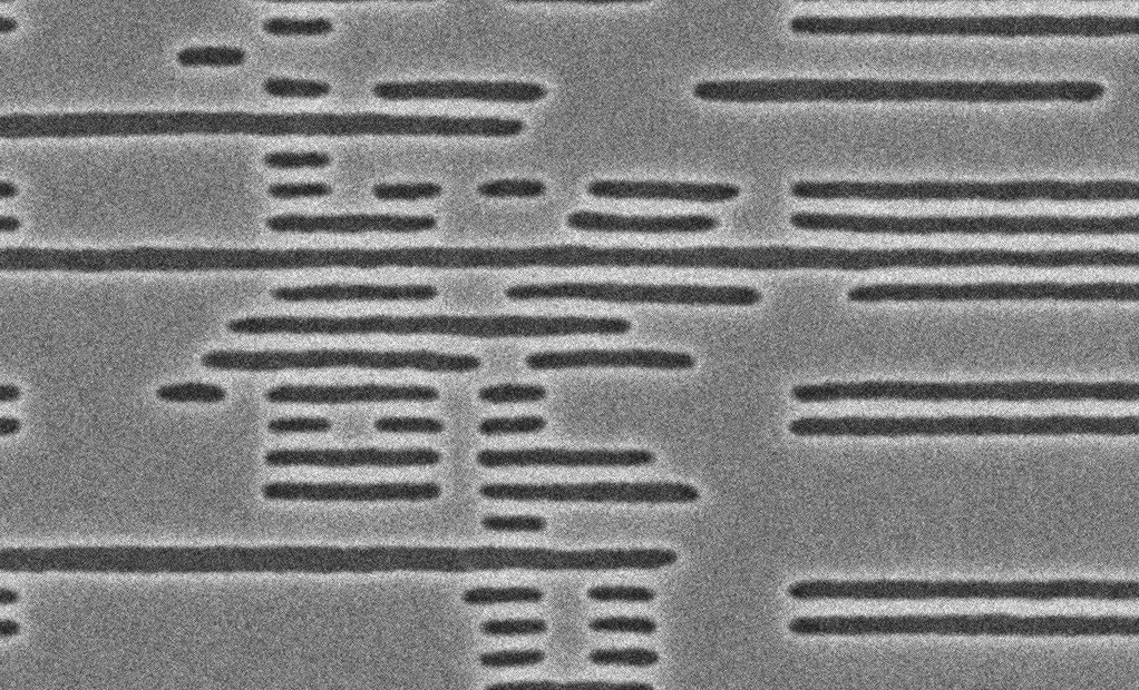
One example is secondary ion mass spectrometry, or SIMS, a technique used to study the composition of material surfaces. Another is scanning probe microscopy, a family of techniques that can measure properties such as topography, adhesion, hardness, chemistry, and electrical behavior at very small scales. Imec’s patented scanning spreading resistance microscopy, or SSRM, is one such technique and allows researchers to determine carrier profiles in semiconductors with nanometer spatial resolution.
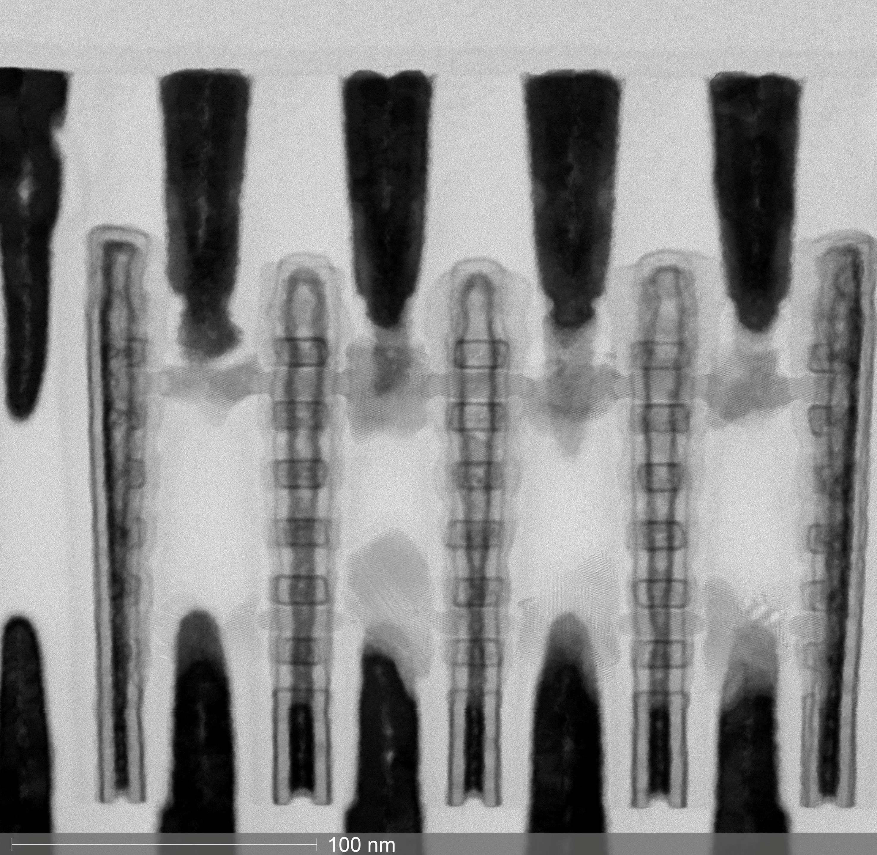
As devices have become smaller and more three-dimensional, metrology has had to evolve as well. Measuring a flat layer is one thing. Measuring confined volumes, nanowires, FinFETs, gate-all-around structures, and tiny embedded features is much more challenging. At these dimensions, the question is not only how to measure more accurately with sufficient spatial resolution, but also how to keep these reduced dimensions measurements statistically still meaningful. The development of array-based metrology such as self-focusing SIMS has been Wilfried’s answer to these challenges.
Hybrid metrology: combining strengths
One of the major trends Wilfried has emphasized is hybrid metrology: combining different measurement techniques on the same structure to obtain richer and more reliable information.
In practice, this means bringing together structural, chemical, and functional measurements. For example, transmission electron microscopy can reveal structure and composition, while scanning probe methods can measure local electrical or functional behavior. By combining these views, researchers gain a clearer understanding of how a device really works.
This approach is increasingly important for advanced semiconductor technologies, where one technique alone is often not enough. The same idea also underpins work on atom probe tomography, atomic force microscopy, in-line characterization, and array-based metrology.
Metrology as a source of value
Wilfried has long argued that metrology should not be seen as a cost factor. Instead, it is a profit center for the semiconductor industry. The reason is simple: better measurement accelerates technology development. It helps researchers understand materials interactions better, detect failures faster, improve processes earlier, and increase yield in manufacturing. Without advanced metrology, the industry cannot reliably move from one technology node to the next.
For imec, this has made metrology a cornerstone of its value to partners. Strong measurement capabilities provide the fundamental insight needed to develop new materials, new devices, and new process flows.
Sharing knowledge across generations
Wilfried’s impact also extends through teaching, publishing, and mentoring. He has co-authored more than 600 peer-reviewed papers, given more than 150 invited presentations, and is co-inventor of more than 60 patents.
Through his long-standing appointment at KU Leuven, he has taught materials characterization and supervised PhD students, helping train generations of researchers in a field that is essential but often less visible than device design or process integration.

Wilfried Vandervorst is a senior imec fellow and professor emeritus at KU Leuven. His work focuses on advanced metrology and material interactions for semiconductor technology, including nanoscale materials characterization, scanning probe microscopy, secondary ion mass spectrometry, ion beam analysis, and electrical characterization of semiconductor structures.
He received his MSc degree in electronic engineering from KU Leuven in 1977 and his PhD in Applied Physics from the same university in 1983. After working at Bell Northern Research in Ottawa, Canada, he joined imec in 1984, where he became director of the materials characterization department. He was elected imec fellow in 2001 and senior imec fellow in 2013.
Expertise
Semiconductor metrology
Nanoscale materials characterization
Scanning probe microscopy and SSRM
Secondary ion mass spectrometry and ion beam analysis
Career highlights
Joined imec in 1984 and helped build its materials characterization expertise
Elected imec fellow in 2001 and senior imec fellow in 2013
Has held a professorship at KU Leuven since 1990
Helped advance semiconductor metrology techniques for increasingly small and complex device structures
Co-authored more than 600 peer-reviewed papers and is co-inventor of more than 60 patents
Has retired at imec in 2019
Published on:
7 September 2026