Semiconductor reliability testing
Imec develops methodologies and tools to model and test semiconductor technologies – from fundamentals to yielding, robust and reliable systems.
Guaranteeing and improving the yield, robustness and reliability of ICs for various applications is an ever-continuing challenge for the semiconductor industry. To help its partners with this task, imec has set up a dedicated expertise center for reliability.
Reliability testing from semiconductor atomic level to system level
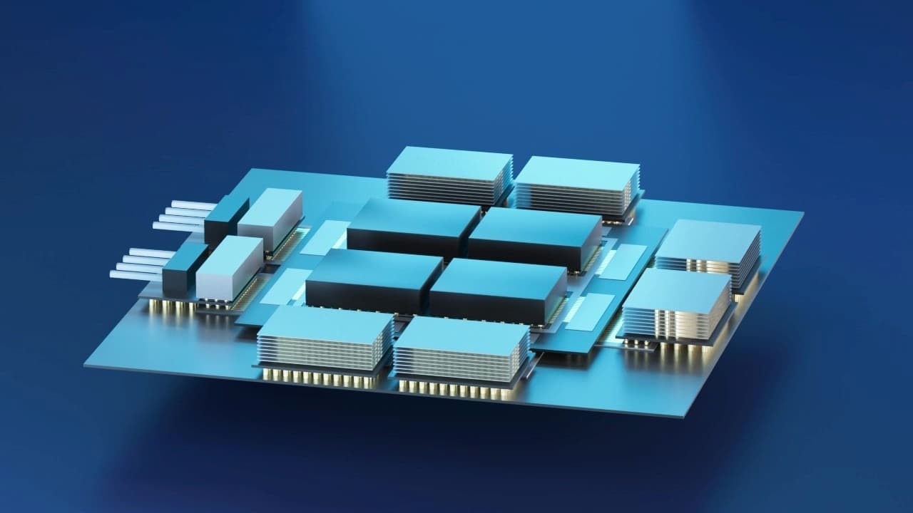
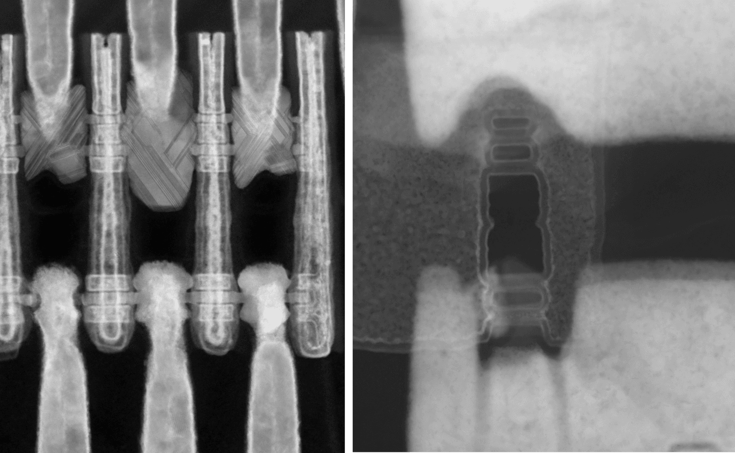
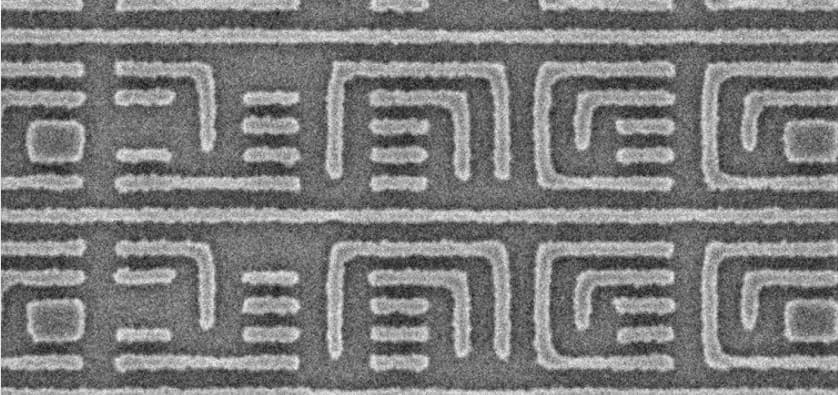
The basis, of course, is to understand what happens when electronics operate properly and when they do not. Our scientists have been studying and modeling this in terms of devices (FEOL), interconnects (BEOL) and packages, sometimes right down to the atomic level, sometimes all the way up to the system level.
Assessing reliability during technology development has become a standard practice. Our work is now also expanding toward the nanoscale level of defect engineering. To this end, our experts are building unique methodologies and tools, which we also provide to our partners.
A system is more than a collection of transistors
More than ever, reliability expertise involves:
- looking at all levels of processing and system design
- using holistic approaches
We no longer look at single transistors but at the behavior of systems made of millions of transistors interconnected and packaged in many different ways.
This approach also includes mechanical and thermal modeling of subsystems, systems and packages. For these, we can design virtual experiments to select the optimal materials, geometries and operational conditions. For some application domains such as automotive and space, these take into account extremely harsh operating and environmental conditions.
The insights gathered from this work allow us to give valuable feedback at various levels:
- To process technologists, to make transistors and their connections more reliable.
- To people involved in DTCO and STCO (design and system technology co-optimization), to improve system reliability at all the abstraction levels, up to the application design.
Imec provides its partners with models, test and characterization methodologies, and software tools they can adopt and use in their R&D. One example is where we enable reliability by design by adding reliability degradation models to compact models and EDA tools. We are also looking at ways to add functional testing and reliability monitoring circuits to system designs.
Our work also includes the optimal design of ESD protections, not as an afterthought added to an already finished design but incorporated from the beginning as part of a reliability-aware technology development.
Semiconductor reliability knowledge as driver for new solutions
One particular aspect of our work, probably unique in the world, is that we are applying our expertise as the basis for innovative and disruptive solutions in very diverse domains.
A most notable domain example is security, where we make use of device degradation physics. As chip degradation is unique to each chip, it can be used to create hardware-based security primitives. One such primitive, for example, is a chip fingerprint, a physically unclonable function (PUF) that uniquely identifies a chip. Others are true random number generators (TRNG) needed in cryptography or odometers to determine the true age of a chip.


