Introduction
Jonathan Borremans (program manager at imec) and Piet De Moor (senior business development manager imagers at imec) present a new approach to charge-coupled-device (CCD)-based time-delay-and-integration (TDI) imaging. The new imager implements the CCD TDI pixels together with advanced CMOS drivers and readout in one single chip. This CCD-in-CMOS technology is compatible with backside illumination for enhanced sensitivity, and multispectral filters can be added for increased imaging performance. With this highly sensitive and high-speed imaging solution, high-end applications such as remote sensing, life sciences and machine vision are targeted.
The principle of time-delayed imaging
Time-delay-and-integration (TDI) imaging is a preferred line-scanning technique used in applications such as industrial inspection and earth observation. In general, this imaging technique can be used when an object or scene is moving linearly over an imager (or vice versa), and when the content of the scene is not changing within a short period of time. Conceptually, a 2D image can be captured by using one linear row of photosensitivity pixels. The image is then taken line by line, delayed in time – the delay being synchronized with the linear scene movement. The resolution is determined by the number of pixels in the row. A smarter way of capturing a 2D image is not to use a single row of photosensitive pixels, but a number of rows. Each row detects the same information as the previous rows, but now delayed in time. By adding the correct scene data of all rows, an increased signal and signal-to-noise can be obtained.
Schematic representation of the time-delay-and-integration principle, using 8 rows of photosensitive pixels
CCD – a ‘noiseless’ way of collecting and transferring the signals
The technology of choice for collecting and transferring the analog TDI pixel data is charge-coupled-device (CCD) technology. CCD uses pixels that can detect light by collecting photon induced charges under a CCD gate – i.e., in a potential well. Interestingly, the collected charge packages can be transferred easily from one gate to an adjacent one, without adding noise. In a TDI implementation, this allows to move a charge packet from one pixel to another (i.e. in a column, along the track) in perfect synchronization with the scene movement. An analogy is often made with the term ‘bucket brigade’, used for a line of people passing buckets of water. As a result, the signal from the different rows (also called stages) at different times are finally collected into the same charge packet. This way, the signal is added in hardware. Importantly, as the charge collection and transfer is noise-free, the only added noise is the one at the final readout stage, when charge is converted into voltage.
A comparison can be made with CMOS imager technology – a technology that is preferred over CCD for consumer imager applications due to its high degree of electronic circuit integration. In a CMOS imager pixel, the light induced signal is converted into the voltage domain, and this step induces a noise increase in each pixel. Contrary to CCDs, when combined with TDI, the signal transfer and the signal storage cannot be done in the charge domain. Rows (or stages) representing the same scene but taken at a different time, are now to be added digitally – in software. This ‘digital TDI using CMOS’ solution not only comes with a noise penalty. It also requires a large memory and fast data processing, as 2D frames are to be read-out at line rate and added in the digital domain. For a large number of TDI rows, this process becomes very complex and power hungry. An advantage of this technology is the high degree of integration, as fast readout electronics can be integrated on the imager chip itself.
TDI CCD-in-CMOS – combining the best of both worlds
Traditionally, a CCD system requires a board with multiple chips, including the CCD, drivers and readout chip. Imec has been developing a new solution that combines CCD pixels and CMOS readout in one technology, enabling a single imager chip with both CCD and CMOS functionality.
This unique technology combines the best of two worlds: the noiseless collection and transfer in charge domain of the CCD technology, and the system integration potential and the low power and fast readout that only CMOS can deliver.
Contrary to traditional imagers that read out pixels per column and multiplex the data to one analog-to-digital convertor (ADC), the new imager uses column-based ADCs. In this configuration, one ADC is used per CCD column, and the different columns are readout in parallel. This results in a high readout rate with low power consumption.
Time delay integration using CCD-in-CMOS
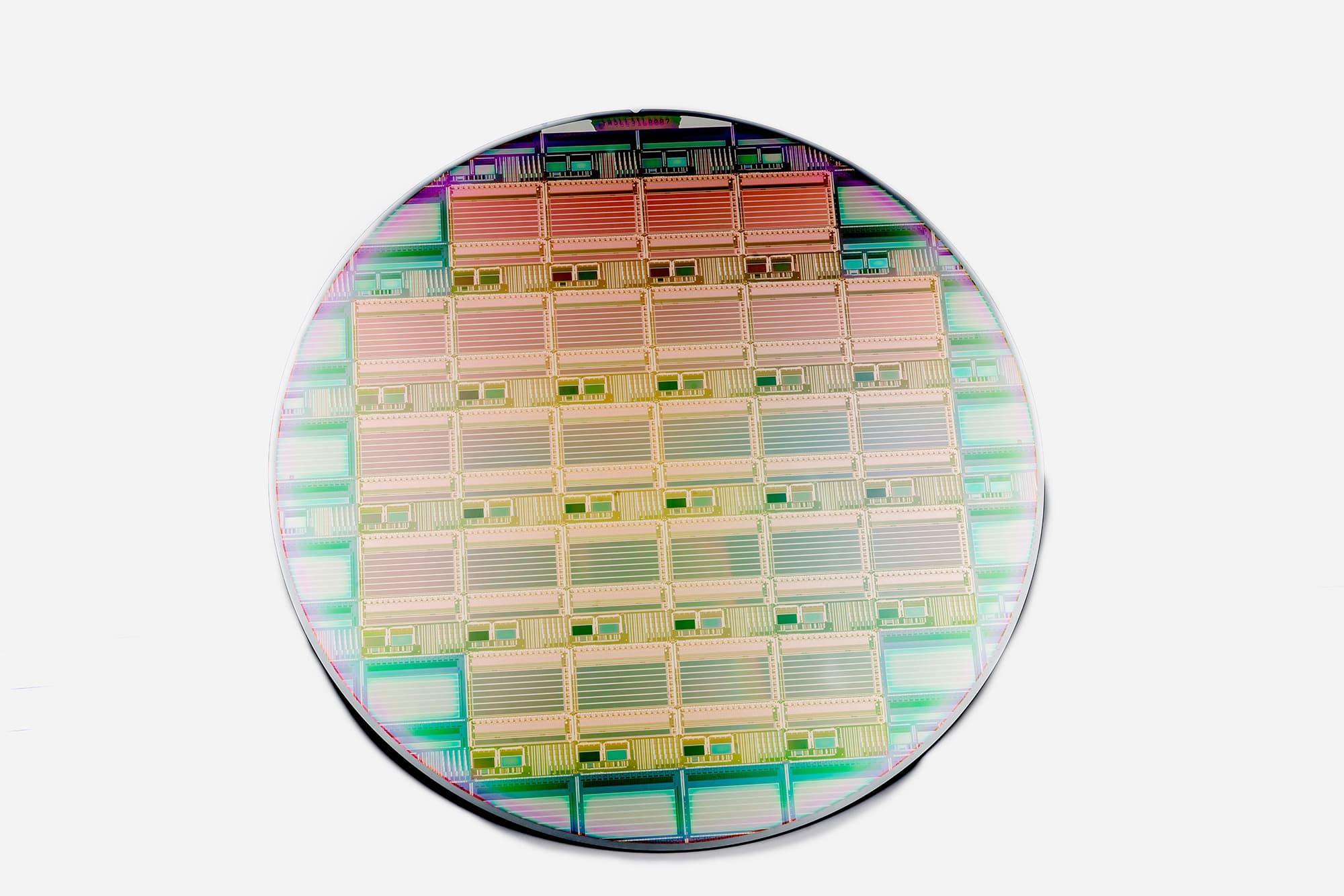
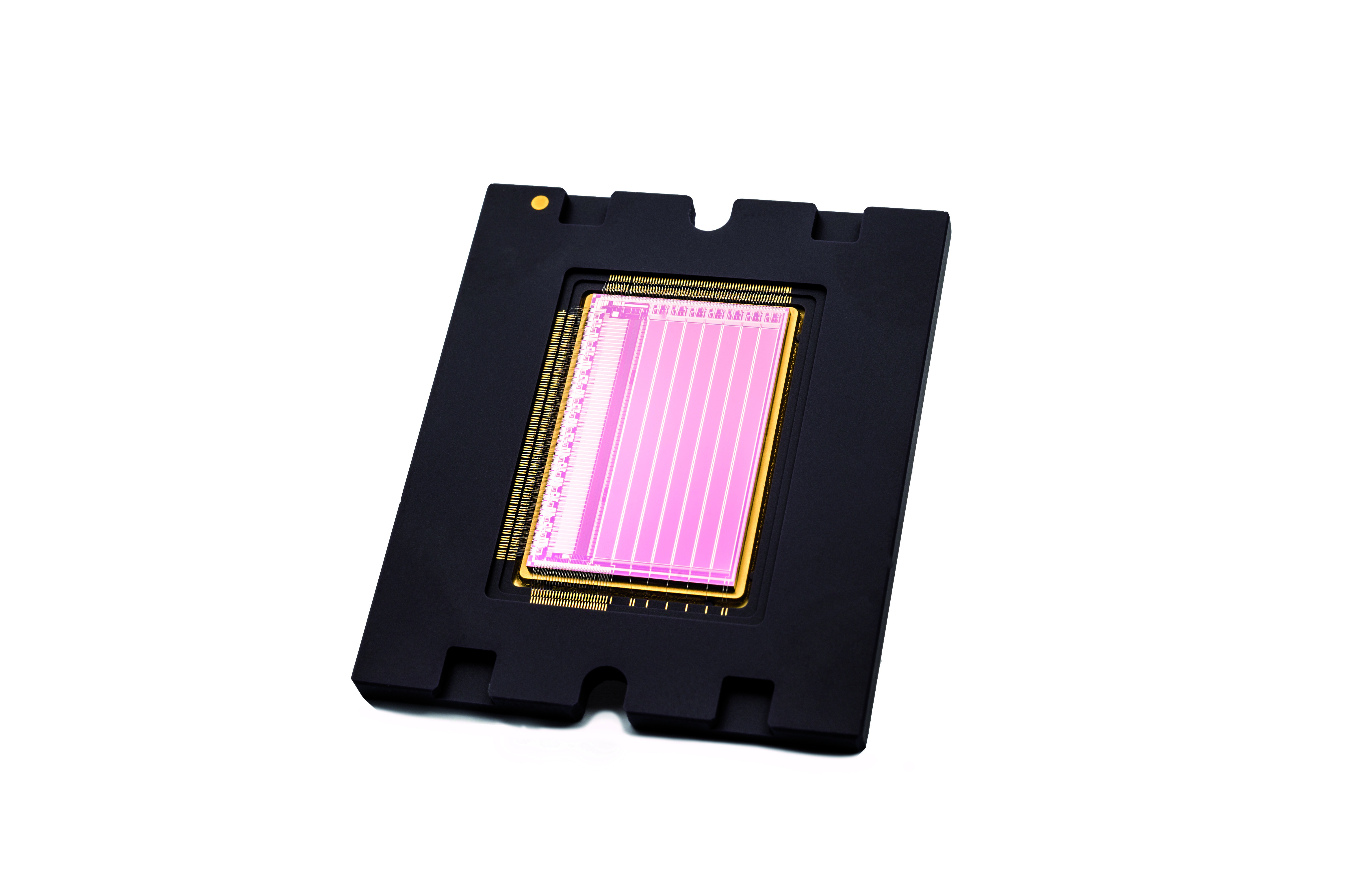
While CCD imagers are typically manufactured on 150mm wafers using dedicated processes, imec has developed a unique CCD process module inside its 130nm CMOS process flow on 200mm wafers. This results in a more cost-effective manufacturing flow. The process is also compatible with other wafer-level post-processing techniques such as backside illumination and spectral filter integration, as well as with CMOS driver and readout circuitry. As part of the CCD process module, narrowly spaced single poly CCD gates are realized above a buried CCD channel. In a final step, the imager sensors are packaged in a ceramic pin grid array (PGA) package.

200mm wafer with CCD-in-CMOS imager

TDI CCD-in-CMOS image sensor
Back-side illumination for maximum sensitivity
In a typical front-side illuminated imager, light enters the optical layers and passes through the so-called ‘back-end-of-line’ layer stack before reaching the light-sensitive silicon. This back-end-of-line consists of metals and dielectric layers, reflecting and even absorbing part of the light. As a consequence, the quantum efficiency of the imager (defined as the overall efficiency of absorbing a photon, transferring it to an electron and collecting the electron) stays well below its theoretical maximum (i.e. 100%). For example, the quantum efficiency for a typical front-side illuminated imager in the yellow/green wavelength range typically reaches about 40%. This can be increased to 70% by using micro-lenses that focus the light.
"A higher quantum efficiency can be obtained by using back-side illumination (BSI). In BSI imagers, the silicon substrate is removed, and light directly enters the imager from the backside. The technology to realize BSI imagers is quite established at imec today."
It consists of bonding the 200mm sensor wafer to a carrier wafer, and then thinning it from the backside. This directly exposes the CCD gates to the light, without obstruction by metal lines or dielectrics. In this configuration, the fill factor (the fraction of the area which is sensitive to light) reaches 100%, and the quantum efficiency is significantly enhanced. Antireflection coatings can be added to reach a high quantum efficiency in selected regions of the spectrum, such as the visible (more than 90% quantum efficiency) or (near-)ultraviolet (70%). And by increasing the final thickness of the Si towards 12 micrometer, the imager can be made sensitive to near-infrared.
Quantum efficiency benefit of using back-side illumination
Spectral TDI sensors
TDI CCD-in-CMOS technology offers a route towards highly sensitive and high-speed imaging solutions. Yet, these imagers represent a scene in black and white.

Imec researchers have gone one step further by adding spectral filters on top of the imager. This enhances the TDI imaging performance and allows to extract significantly more features from a scene than a traditional solution.
To meet the demand for spectrally resolved imaging, imec has been developing a process module that allows the post-processing of hyperspectral filters (up to 256) on top of (e.g. commercial) CMOS imagers. By applying different designs, a multitude of hyperspectral imaging concepts can be created and the trade-off between spatial and spectral resolution can be optimized for a given application. For certain applications, it would make sense to combine this hyperspectral technology with TDI CCD-in-CMOS technology. However, there is a fundamental incompatibility. Multiple spectral filters are placed over a TDI imager. Using the TDI mechanism, the individual filtered signals for each row will be added. This way, the individual spectral information taken by the different filters gets lost, thereby failing to achieve its aim of collecting spectral information. This can be solved by designing different TDI arrays with each their own readout, where the conversion of charge to voltage is done. Using the CMOS electronics, it is then possible to use one common readout block to read out multiple TDI arrays at high speed.
"A TDI imager has been developed with 7 bands allowing the integration of up to 7 spectral filters on top. This 7-band version contains 7 CCD arrays of each 4,096 x 256 pixels."
Interestingly, the imager can be made reconfigurable: the number of active bands as well as the number of stages per band (1-to-256 per band) can be chosen. Some filters may transmit less light than others which can be compensated for by reconfiguring the device. The chip integrates 4,096 column ADCs and 32 digital data transmitters capable of operating at 1Gbps. A line rate of up to 300kHz is targeted, corresponding to 57kHz per band when all bands are enabled. The charge transfer efficiency, measured per column, is greater than 0.99995 up till 300kHz. Today, the spectral filters are added on a glass lid. In the near future, wafer-level processing of the spectral filters will become possible.
(Left) Schematic representation and (right) photograph of imec’s multispectral TDI with 7 bands
A growing number of applications
One of the first markets that made use of TDI-based cameras is earth observation from space. In these applications, large satellites move in low orbits, resulting in a linear movement of the camera with respect to the ground. TDI is a very useful technique for earth observation applications, as it increases the signal-to-noise ratio of the detected images. CCD-based TDI results in a signal-to-noise increase up to a factor equal to the number of TDI rows. By combining this technology with advanced CMOS readout electronics, the system complexity and size is drastically reduced, making the technology suitable for implementation into small satellites and even drones. In earth observation, there is also a tendency to use spectrally resolved imaging and hyperspectral imaging. The combination of both spatial and specific spectral signature of objects is particularly interesting for environmental monitoring, precision agriculture, disaster detection and monitoring, etc.
"A second market is industrial machine vision where typically products are moving linearly on a conveyor belt. Examples are flat panel inspection, semiconductor front-end inspection, printed circuit board inspection, glass inspection etc. For these applications, the high scanning speed of the imager is a key characteristic."
There is also a broad interest in using multispectral TDI cameras, even hyperspectral cameras. They allow to take full images at every single wavelength of interest over very large areas and produce lots of data at very high speed. A typical application that benefits from these characteristics is banknote inspection.
An emerging application field is life sciences, where massive amounts of cells or tissue need to be scanned at a very high speed. Potential applications include DNA sequencing, or cell cytometry involving the movement of cells in a microfluidic channel. The TDI CCD-in-CMOS imager can for example be combined with imec’s cell sorter to detect circulating tumor cells. The imager can be deployed to image, reconstruct and sort the cells that move at about 1m/s. Another potential application is slide imaging for diagnostic purposes in pathology.
Conclusion
Imec has realized a TDI imager using CCD-in-CMOS technology, thereby exploiting the noiseless charge transfer of CCD with the efficiency of CMOS high speed drivers and readout. The sensors can be produced in a CMOS-compatible flow, resulting in a simple and cost-efficient solution. The sensitivity of the imagers can be increased by using back-side illumination, and the TDI imaging performance can be enhanced by adding multispectral or hyperspectral color filters. Today, the multispectral color filters are added on a glass lid. Work on the wafer-level processing of the filters is currently ongoing. Imec also works on an increased number of bands and columns, enabling a higher spatial and spectral resolution.
"Imec offers the specialty imagers through various business models, ranging from full-custom design to off-the-shelf prototype TDI sensors and evaluation cameras."
The prototype TDI sensors use a format with 4,096 columns and 256 stages per CCD array (or band). A version with one CCD array is available, as well as a 7-band version, allowing to add 7 spectral filters.
This project has received funding from the Electronic Component Systems for European Leadership Joint Undertaking under grant agreement No 662222. This Joint Undertaking project ‘EXIST’ receives support from the European Union’s Horizon 2020 research and innovation programme and Belgium, Netherlands, Greece, France.
Want to know more?
- Send an email to imecmagazine@imec.be to receive the paper ‘A 7-band CCD-in-CMOS multispectral TDI imager’, D. San Segundo Bello et al., 2017 International Image Sensor Workshop, May 30th – June 2nd, Hiroshima, Japan
Jonathan Borremans received the M.Sc. and Ph.D. degree in Electrical Engineering at the University of Brussels, in collaboration with imec, Belgium. He authored more than 80 papers and patents. He joined imec’s wireless group, leading the CMOS reconfigurable receiver research, and consulting for cross-disciplinary projects (including MEMS-CMOS based systems) as a circuit- and system architect and Principal Scientist. Currently, as a Program Manager, he leads the imager design group at imec.
Piet De Moor received his PhD in Physics from University of Leuven in 1995. After joining imec in 1998 he consecutively lead different sections and groups in the areas of MEMS packaging, 3D Integration and Pixel Design and Test. The last years he was Program Manager Imagers. He has been technically coordinating several bilateral, EC, ESA, and nationally funded projects on advanced imaging systems. Recently he is appointed senior business development manager imagers.
Published on:
26 September 2017


