
CFET technology moving forward, backed by integration efforts and DTCO studies
The semiconductor industry is going through a major architectural transition, with gate-all-around (GAA) nanosheet transistors replacing FinFETs in advanced logic nodes of 3nm and beyond. GAA nanosheet transistor technology offers scalability down to the A10 logic generation, where it enables 5.5-track (T) standard cells – the track being a measure for the standard cell height.
For the A7 node, options are becoming increasingly diverse to meet the growing diversification of application needs, driven by the AI revolution. According to imec’s latest roadmap, one option is to design systems around imec’s CMOS 2.0 scaling paradigm. With CMOS 2.0, a system-on-chip (SoC) is partitioned into heterogeneous, functional tiers each optimized using the most suitable technology, and reconnected using 3D interconnect technologies. For other use cases, GAA nanosheet technology may be pushed to its ultimate scaling limits, with power delivered from either the frontside or the backside. But industry may as well transition to complementary FET (CFET) device architectures. By stacking p and nMOS transistors on top of each other, standard cells can be further scaled down to 3T, thereby extending the classical CMOS logic roadmap to at least the A3 technology node.
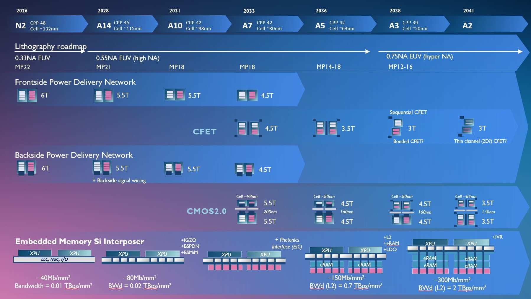
Figure 1 – Imec’s logic technology roadmap.
Imec and its industrial partners are working to make CFET-based devices manufacturable. In recent years, they laid the groundwork for key integration approaches, categorized as monolithic CFET (mCFET) and sequential CFET (sCFET) [1,2].
Both approaches start from the vertical stacking of Si/SiGe layers from which the n and pFETs are fabricated. With mCFET, the vertical device structure with common top and bottom gates is patterned and processed in a single sequence of process steps. The patterning, deposition and selective removal of materials around and in between the high-aspect ratio device structure requires considerable effort in terms of module development. sCFET, on the contrary, patterns the top and bottom devices independently using dedicated masks. With sCFET, the individual process steps are simpler compared to mCFET but some critical steps need to be executed twice – for top and bottom separately. sCFET additionally involves two wafer flips, distorting the wafer and challenging the precise alignment of front-to-back device connections. Pending further progress in alignment accuracy, mCFET is believed to offer the fastest path to industrial adoption.
Progress in CFET integration is complemented with design-technology co-optimization (DTCO) studies that examine CFET device architectures from a circuit level perspective [2]. These studies aim to identify scalable standard cell configurations and performance boosters that offer the best tradeoff in terms of power, performance, area and cost.
In this 2-part article, we report major progress in CFET device integration, and we discuss CFET scalability using DTCO studies.
In part 1, two process modules were presented that are essential for both mCFET and sCFET device flavors: (1) a backside contact module, and (2) a gate stack integration approach that enables multiple threshold voltages (Vt) in nanosheet and CFET devices.
In part 2, a scalable architecture for sCFET is introduced, allowing both split-gate and common-gate configurations. Besides progressing the logic roadmap, DTCO work shows how this split-gate architecture also benefits CFET-based SRAM scaling. Finally, improved back-end-of-line (BEOL) routability is demonstrated, supporting the scaling of CFET standard cells.
The reported results are achieved in the framework of the imec-hosted European NanoIC pilot line, which is targeting the development of beyond-2nm systems-on-chip. CFET development, which is centered on CFET-specific designs, process steps, modules and baseline flows, has been selected as one of the key enabling technologies for extending the logic roadmap into the ångström era. This will help Europe to remain at the forefront of next-generation semiconductor innovation and manufacturing.
A novel architecture for sCFET: split-gate device architecture enlarges CFET’s scaling potential
Earlier DTCO studies have already demonstrated the scaling potential of CFET technology across subsequent logic nodes – a prerequisite for the semiconductor industry to adopt the new device architecture. For mCFET, for example, imec previously identified the double-row (DR) CFET architecture as the most optimal way to integrate mCFETs into an A7 standard cell [3]. A double-row CFET standard cell contains two rows of stacked devices with a shared vertical signal via in between, and power walls at the cell boundary (see Figure 2). Later, layout inefficiencies were addressed, resulting in an optimized version of the double-row CFET: the half-height double-row (hDR) architecture. At IEDM 2025, additional scaling boosters such as the integration of hybrid channels were introduced to support aggressive area scaling targets towards A3 [2].
Common-gate and split-gate devices: the challenge of offering both flavors with one device architecture
The process flow for fabricating mCFET devices inherently offers common-gate devices: the gates of n and pFETs are structurally connected to one another. This works well for 90-95% of all basic logic gates – think about an inverter circuit (or NOT gate) that performs the logical operation of negation. But for other logic circuits, such as flipflops and multiplex gates, independent control of n and pFET metal gates is desired. One way to address this need is to leave one polarity of the stacked CFET device unused (for example, only using the nFETs, and removing the pFETs). While this approach solves the gate control issue, it does not fully exploit the area benefit of stacking n and pFETs.
sCFET device architectures, where top and bottom devices are patterned independently, can offer split-gate devices in a more natural way. But conventional sCFET architectures leave us with the opposite problem: an extra module is needed to connect the gates for those circuits that need it.
A double-flip sCFET architecture: offering both options in an area efficient way
At 2026 VLSI, imec introduces the double-flip sCFET architecture that offers both split-gate and common-gate device options without compromising area efficiency [4].
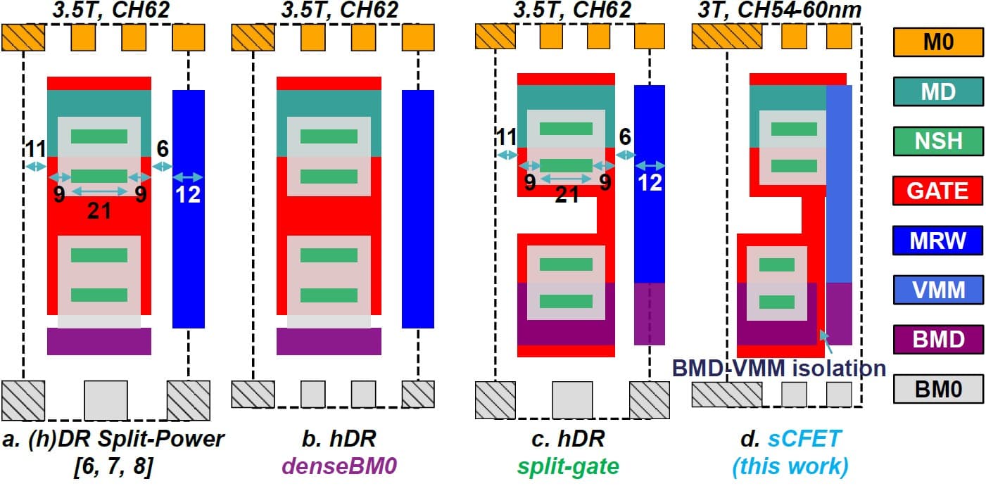
Figure 2 - Cross-sectional views of (a) double-row mCFET (DR), (b) half-height double-row (hDR) with dense backside metal-0 tracks (BM0), (c) hDR with split gate, and (d) sCFET with split-gate and dense BM0 (as presented at 2026 VLSI). (CH = standard cell height; NSH = nanosheet channels; MRW = shared signal wall; VMM = via that can bypass the bottom device; MD = metal-to-diffusion layer)
The impact of the new architecture in terms of area efficiency and routability was evaluated for various CFET-based libraries, designed around, for example, AND, OR and inverter circuits. With an overall library efficiency (η) as high as 98%, the new sCFET double-flip architecture provides the most efficient area utilization compared to double-row (DR) and half-height double-row (hDR) mCFET architectures. When combined with dense backside metal-0 (BM0) routing, the new architecture supports 3T standard cells that will be needed in A3 and A2 logic nodes – according to imec’s latest technology roadmap.
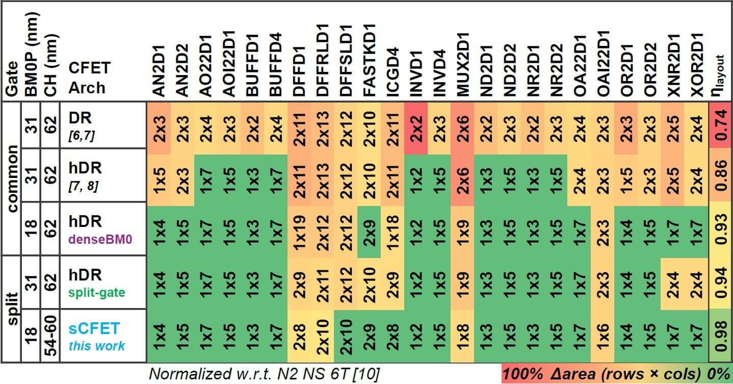
Figure 3 – Cell area breakdown of CFET libraries, for each of the CFET architectures (double row (DR), half-height double-row (hDR), hDR with dense backside metal-0 routing (hDR/dense BMO), and double-flip sCFET). sCFET significantly optimizes cell library and achieves an overall 98% layout efficiency (hlayout) (as presented at 2026 VLSI).
The double-flip sCFET flow starts from a bonded stack with an embedded middle dielectric isolation (eMDI) between top and bottom devices [2]. First, the top device is patterned from the frontside, and the top gate is finished partly during the replacement metal-gate module. After wafer flip and wafer thinning, the bottom device is patterned from the backside. Next, a via connection between bottom and top gate is optionally provided, which can be utilized for common-gate use cases. Following a second wafer flip, processing of the top and bottom devices is completed.
Additional scaling potential is offered by the possibility to introduce hybrid channels, optimized for n and pFETs separately. Think about CFET devices with different channel orientations for the top and bottom devices, or CFETs with asymmetric sheet widths. This brings along extra power-performance-area benefits and supports design flexibility.
A 5T+1 CFET SRAM bit cell: split-gate sCFET device architecture prolongs the SRAM scaling roadmap
Static random-access memory (SRAM) continues to be industry’s main workhorse for providing on-chip cache memory – the high-speed memory that interfaces between dynamic RAM (DRAM) and XPU. A conventional SRAM memory bit cell consists of six transistors: four nFETs and two pFETs (or, alternatively, two nFETs and four pFETs). Of these FETs, two nFETs and two pFETs (PUx and PDx in Figures 5 and 6) are paired to form two cross-coupled inverters, able to store one bit of information. The remaining nFETs are designed as pass-gate transistors (PGs), connecting to the bit and word lines (BL, WL) and controlling the data flow during the read and write operations.
The SRAM density crisis: can CFET bring relief?
Just as in logic technology, the density increase of SRAM memory relies on dimensional scaling of the bit cells, in combination with device architecture innovations. But since the 7nm technology node, SRAM bit cell scaling has fallen flat compared to logic CMOS device scaling. This asymmetry in scaling potential presents considerable challenges for chip designers. Even the transition to GAA-nanosheet-based 6T SRAM cells could not provide the required power, performance, and area benefits. CFET-based 6T SRAM technology is expected to bring initial relief, as the stacking of (part of) the n and pFETs (i.e., PUx and PDx) can substantially increase the SRAM bit cell density.
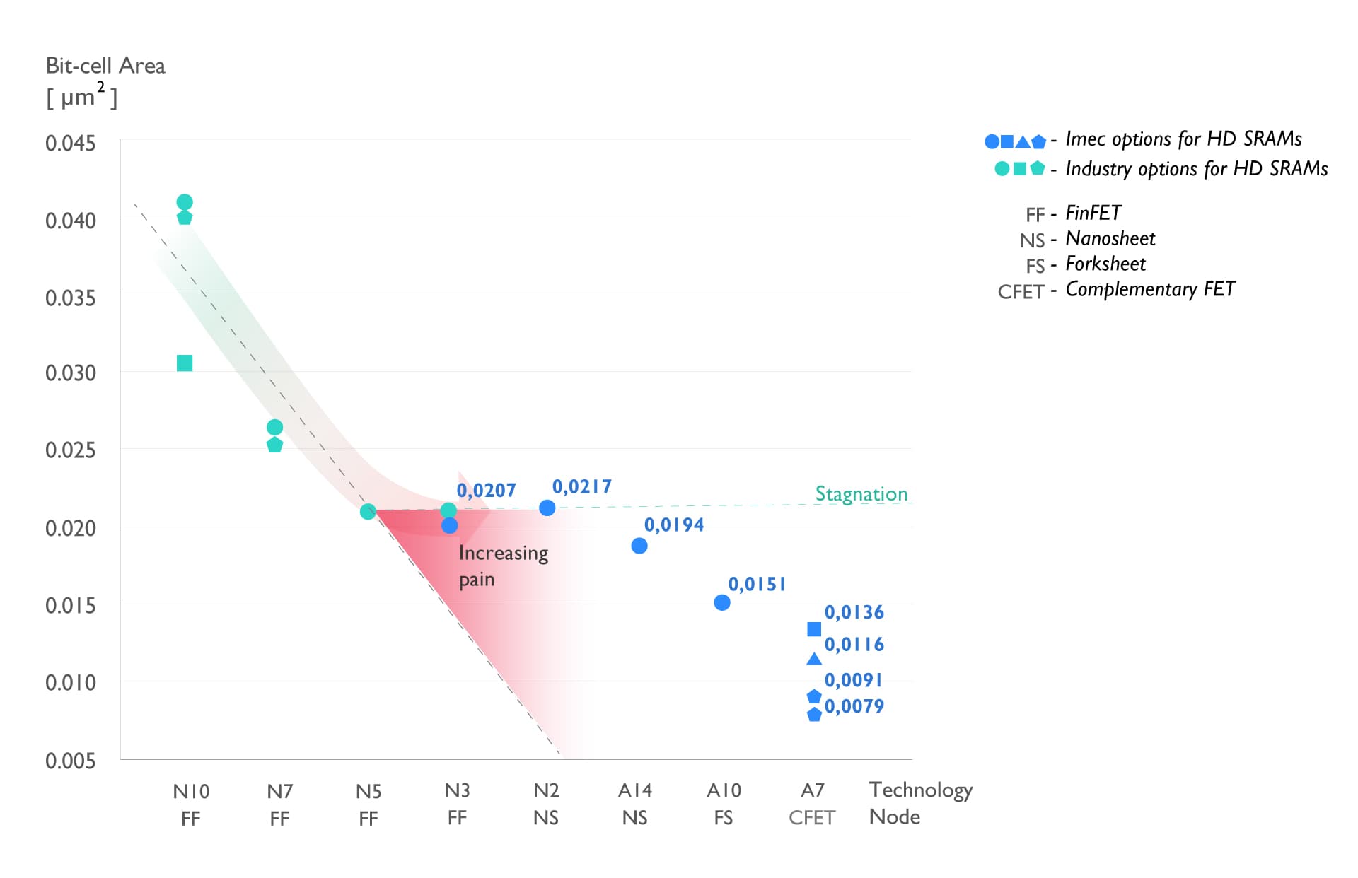
Figure 4 – The SRAM density crisis. The blue symbols represent imec’s options for high-density SRAMs, including single row, double-row, optimized double-row, and the new 5T+1 architecture (as presented at 2026 VLSI).
But even in the CFET SRAM era, further area reduction is being challenged, as the 6T SRAM bit cell does not map efficiently onto a CFET-based architecture. While the two inverters can be mapped using a stacked n/p device architecture (PUx and PDx), the two nFETs serving as the single pass-gate transistors (PGs) leave the two top p-type transistors of the CFET device stack unused. As a result, the intrinsic vertical density advantage of CFET cannot fully translate into bit cell area scaling for a 6T SRAM. A 5T SRAM bit cell configuration with only one single pass-gate transistor has been investigated as an area-efficient alternative, but writability and noise issues have challenged its adoption.
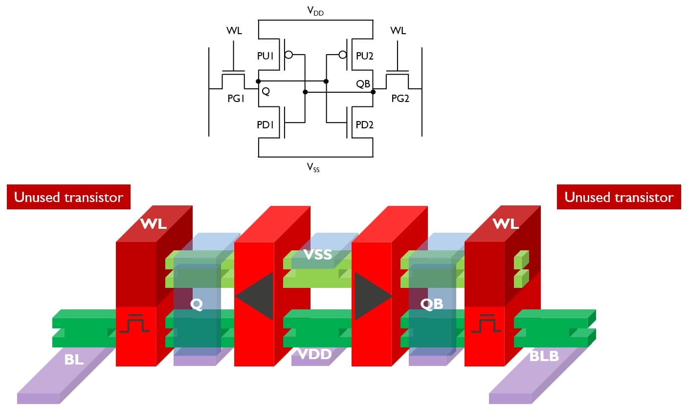
Figure 5 - Schematic representation of a conventional 6T SRAM, which does not map nicely onto a CFET (as presented at 2026 VLSI). (WL = word lines; BL and BLB = bit lines; PUx and PDx form the cross-coupled invertors storing 1 bit of information; VSS and VDD are power supply lines)
A promising 5T+1 SRAM CFET architecture: enabled by sCFET split-gate devices
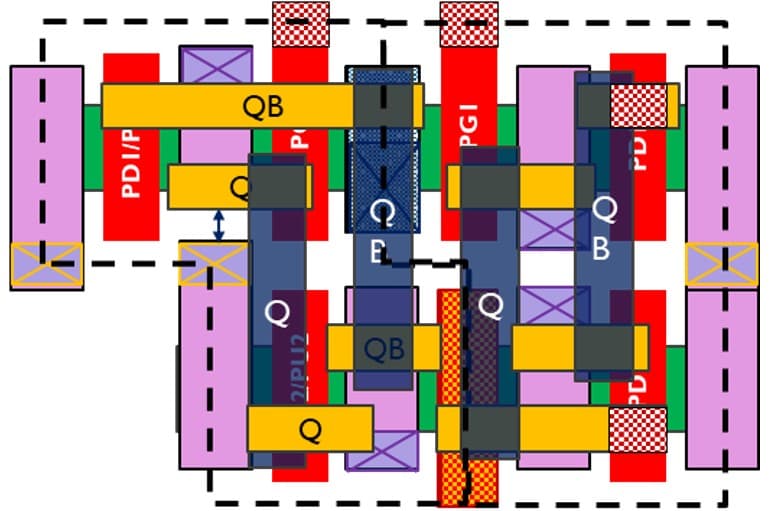
Imec’s novel sCFET architecture for split-gate devices now opens doors to continued SRAM density scaling – as presented at 2026 VLSI [5]. In a novel 5T+1 architecture, the two single pass-gate transistors (PGs) are replaced with one CFET transmission-gate device (TG) that pairs an nFET and a pFET. Such a transmission gate needs independent n and p gate control, which can be enabled by implementing imec’s novel sCFET split-gate device. As such, a 5T-like SRAM bit cell (i.e., a single-ended SRAM bit cell with sCFET transmission gate) can be realized while maintaining a 5T footprint. The use of the transmission gate as the access device also improves writability compared to a ‘classic’ 5T implementation.
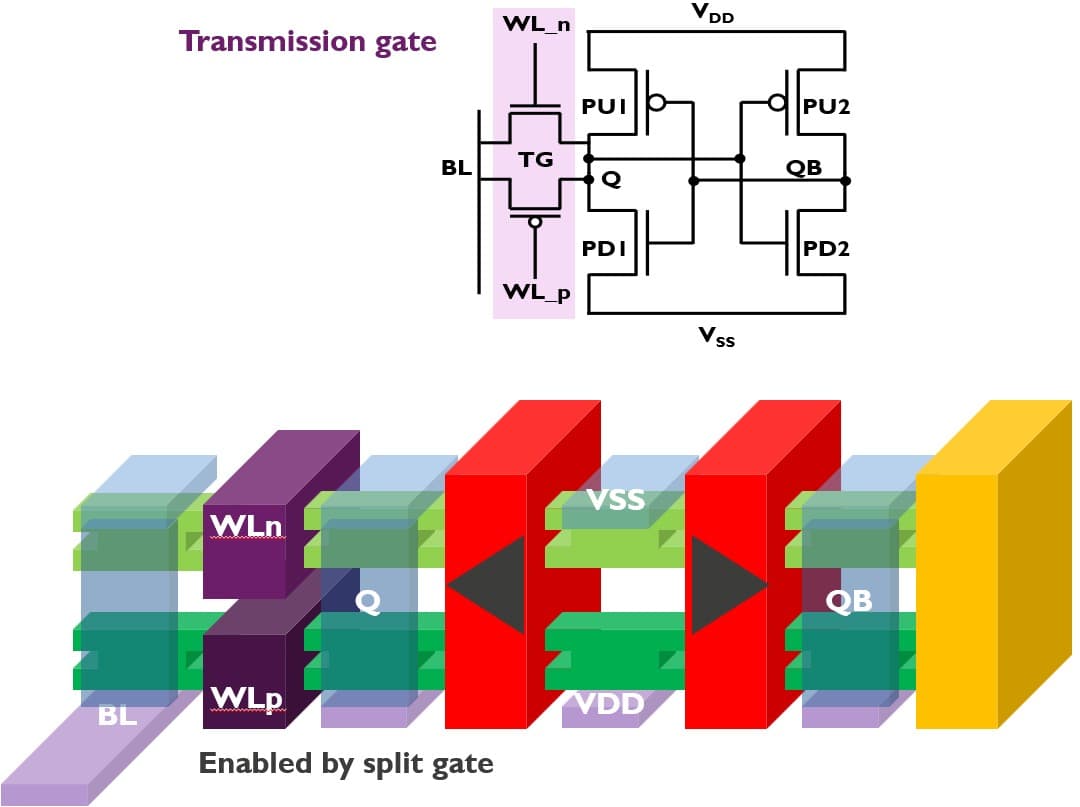
Figure 6 – Schematic representation of a 5T+1 CFET SRAM with transmission gate (as presented at 2026 VLSI). (BL = bit line; WLn and WLp are word lines connecting to the n and p FETs of the transmission gate (TG); VSS and VDD are power supply lines)
SRAM operation can be further improved by optimizing layout and routability at the memory array level. By using this innovative 5T+1 configuration, imec’s DTCO study shows a 12.5% smaller bit cell compared to a conventional 6T CFET SRAM cell, with 7-15% faster write operation. This makes the 5T+1 CFET SRAM bit cell an attractive option for prolonging the SRAM scaling roadmap towards A7 and beyond.
Beyond standard cells: improved BEOL routability to support the CFET scaling roadmap
In various DTCO studies, imec has demonstrated the ability to scale CFET device architectures across subsequent logic technology nodes, supported by innovative standard cell configurations and scaling boosters. But as we approach the ångström era, the area advantages at standard cell level can easily be undone by scaling issues in the BEOL, following a new DTCO study presented by imec at 2026 VLSI [6]. In other words: it becomes increasingly difficult to interconnect the various CFET-based standard cells.
Under the ideal scaling scenario where everything scales proportionally, routability stays the same from one node to another. However, starting from the 2nm node, the scaling of some of the ground rules such as the contact poly pitch (CPP, a metric determined by both the gate length and source/drain contact length) and metal-1 pitch has started to slow down. And this increases routing congestion in the wafer frontside, which affects performance, power and area. In addition, aggressive standard cell scaling limits accessibility to the input and output pins.
Increasing the gear ratio: improved BEOL routability for CFET-based ångström node technology
Fortunately, there are several knobs for improving the BEOL routability. One of these is enhancing the so-called gear ratio, which represents the ratio of the CPP to the metal-1 pitch. In 2nm node processor designs, this gear ratio is usually around 1:1. At 2026 VLSI, imec demonstrated through a DTCO study that increasing the gear ratio to 2:1 for A7 CFET-based designs can improve both pin accessibility and area utilization, without compromising power and performance [6]. In practice, this will drive the metal 1 to smaller pitches, requiring more advanced lithography options like single-patterning High NA EUV lithography for its fabrication.
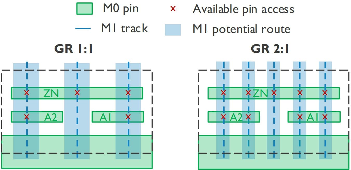
Figure 7 – Schematic representation of M1 routing for ND2D1 cells in A7 with GR 1:1 and GR 2:1, showing improved pin accessibility for GR 2:1 (as presented at 2026 VLSI).
Wrapping up Part 2: enabling the CFET scaling roadmap
With the double-flip sCFET, imec is introducing a new CFET device architecture into the logic roadmap. Double-flip sCFET has a high scaling potential, offering both split-gate and common-gate device options without area penalty. The novel architecture not only benefits the logic roadmap, but it also provides a solution for the stalled SRAM roadmap by enabling a 5T+1 SRAM CFET bit cell memory. In another DTCO study, imec shows how improved BEOL routability can further support the aggressive scaling of CFET based standard cells.
This work has been enabled in part by the NanoIC pilot line. The acquisition and operation are jointly funded by the Chips Joint Undertaking, through the European Union’s Digital Europe (101183266) and Horizon Europe programs (101183277), as well as by the participating states Belgium (Flanders), France, Germany, Finland, Ireland and Romania. For more information, visit nanoic-project.eu.
This article was originally published in Semiconductor Engineering
Want to know more?
[1] ‘Towards a process flow for monolithic CFET transistor architectures,’ imec reading room, 2023;
[2] ‘Performance boosters to scale monolithic CFET across multiple logic technology nodes,’ S. Yang et al., imec Reading Room, 2025;
[3] ‘Imec proposes double-row CFET for the A7 technology node,’ imec Press Release, 2024;
[4] ‘Double-flip sequential CFET: superior 3T library efficiency and PPA,’ S. Yang et al., 2026 VLSI;
[5] ‘5T+1 CFET SRAM with dual-bitline-per-cell-height enabling differential readout and 12.5% area reduction,’ D. Abdi, 2026 VLSI;
[6] ‘Scaling high density designs towards Angstrom nodes: BEOL routability, pin accessibility challenges and impact of gear ratio,’ J.-Y. Lin, 2026 VLSI.